Thin film packaging method and structure

A technology for thin film encapsulation and encapsulation of devices, which is applied in the manufacture of electrical components, electric solid-state devices, semiconductor/solid-state devices, etc. The effect of improving the bending resistance and reducing the deviation of the thermal expansion coefficient

Inactive Publication Date: 2017-01-04
KUNSHAN NEW FLAT PANEL DISPLAY TECH CENT
View PDF10 Cites 26 Cited by
  • Summary
  • Abstract
  • Description
  • Claims
  • Application Information

AI Technical Summary

Problems solved by technology

The water and oxygen barrier effect of the ALD film layer is the best, but because the density and stress of the ALD film layer are relatively large, and the the

Method used


Image

  • Thin film packaging method and structure
  • Thin film packaging method and structure
  • Thin film packaging method and structure

Examples


preparation example Construction

[0052] In this application, the preparation methods of the inorganic layer and the organic material layer are all prepared by existing methods.

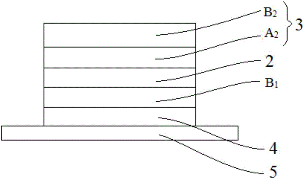
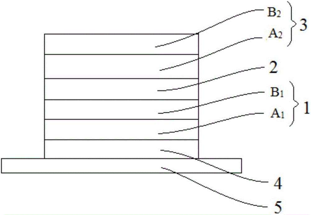
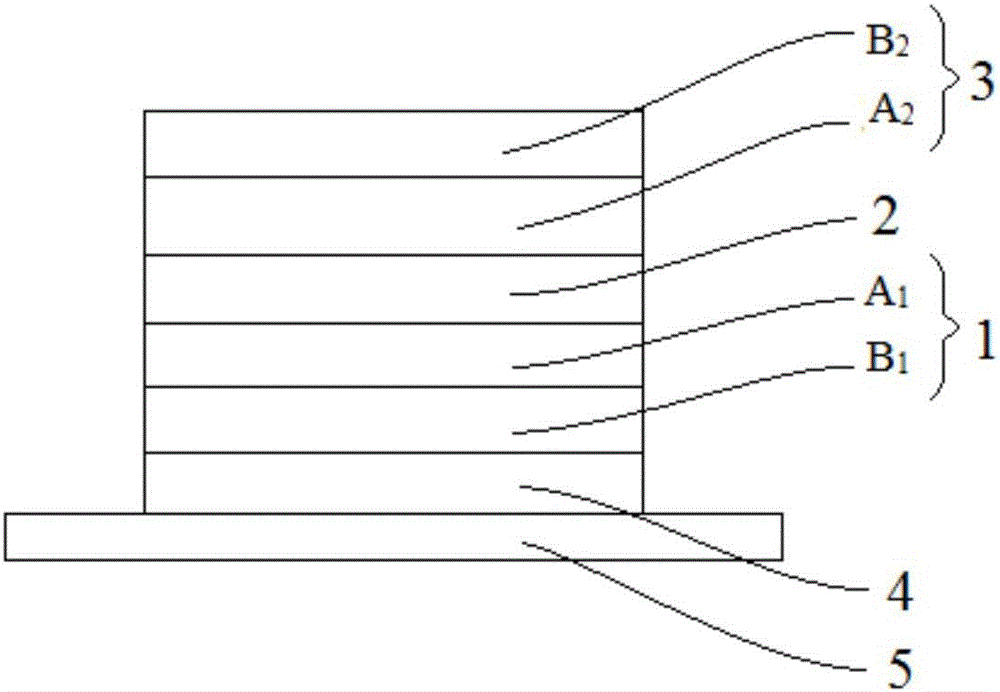
[0053] The present application also relates to a thin-film packaging structure. The thin-film packaging structure is arranged on the surface of the packaging device. The surface of the packaging device is sequentially provided with a first inorganic material layer, an organic material layer and a second inorganic material layer. The first inorganic material layer and the second The inorganic material layer includes an inorganic layer B prepared by atomic layer deposition, and at least one surface of the inorganic layer B is provided with an inorganic layer A prepared by physical vapor deposition or chemical vapor deposition.

[0054] As an improvement of the thin film packaging structure of the present application, the material of the inorganic layer B prepared by atomic deposition is the same as that of the inorganic layer A prepared...

Embodiment 1

[0061] A thin-film encapsulation structure comprising a first inorganic material layer 1, an organic material layer 2 and a second inorganic material layer 3 from the OLED surface upwards, the specific structure, material and thickness of which are shown in Table 1;

[0062] Table 1:

[0063]

[0064] Among them, 0

[0065] Preparation Process:

[0066] First, the top-emitting OLED device and the driving backplane are prepared, and the device to be packaged is placed in a physical vapor deposition equipment, and an aluminum target is used to deposit the inorganic layer A by reactive sputtering 1 , the deposition thickness is 80nm; after the deposition is completed, it is sent to the atomic layer deposition equipment, and the precursors are trimethylaluminum TMA and H 2 O, the precursor reacts to form the inorganic layer B 1 , the deposition thickness is 50nm; repeat the physical vapor deposition process, and then deposit 80nm thick AlO x as an inorganic layer C ...

Embodiment 2

[0070] A thin-film encapsulation structure comprising a first inorganic material layer 1, an organic material layer 2 and a second inorganic material layer 3 sequentially from the surface of the OLED, and its specific structure, material and thickness are shown in Table 2;

[0071] Table 2:

[0072]

[0073]

[0074] Among them, 0

[0075] Preparation Process:

[0076] First, prepare the top-emitting OLED device and the driving backplane, place the device to be packaged in a chemical vapor deposition equipment, use silane and laughing gas as the reaction gas, and react to form an inorganic layer A 1 , the deposition thickness is 100nm; after the deposition is completed, it is sent to the atomic layer deposition equipment. The precursor is tetraethyl orthosilicate and oxygen, which react to form the inorganic layer B 1 , the deposition thickness is 50nm; repeat the chemical vapor deposition process, and then deposit 100nm thick SiO x as an inorganic layer C 1 , a...


PUM

PropertyMeasurementUnit
Thicknessaaaaaaaaaa
Thicknessaaaaaaaaaa
Thicknessaaaaaaaaaa

Abstract

The application relates to the technical field of display, and particularly relates to a thin film packaging method and structure. The thin film packaging method disclosed by the application at least comprises the following steps of: sequentially preparing a first inorganic material layer, an organic material layer and a second inorganic material layer on the surface of a device to be packaged, and when the first inorganic material layer and/or the second inorganic material layer is prepared, firstly, preparing an inorganic layer A by adopting a physical vapor deposition method or a chemical vapor deposition method, and then preparing an inorganic layer B on the surface of the inorganic layer A by adopting an atomic layer deposition method; or, preparing the inorganic layer B by adopting the atomic layer deposition method, and then preparing the inorganic layer A on the surface of the inorganic layer B by adopting the physical vapor deposition method or the chemical vapor deposition method. According to the thin film packaging method and structure disclosed by the application, a composite inorganic layer prepared by utilizing the physical vapor deposition method or the chemical vapor deposition method and the atomic layer deposition method is gradually varied in density, so that a deviation of coefficients of thermal expansion of the prepared inorganic layer and organic material layer is reduced, and bending resistance of a display screen is improved.

Description

technical field [0001] The present application relates to the field of display technology, in particular, to a thin film packaging method and its structure. Background technique [0002] Electronic devices, especially organic electronic devices, are particularly sensitive to moisture and oxygen in the air, so organic devices need to be packaged to ensure the performance and service life of the device. At present, the main method of flexible organic electronic device packaging is to directly fabricate a flexible film structure with excellent water and oxygen permeability on the surface of the device. Since the flexible polymer film has a very limited ability to block water and oxygen penetration, while the dense and pinhole-free inorganic film has a high ability to block water and oxygen, but when it reaches a certain thickness, it shows a rigid structure and is easily broken. Most of the flexible packaging research is carried out based on the packaging technology of organic...

Claims


Application Information

Patent Timeline
IPC IPC(8): H01L51/52
CPCH10K50/844
Inventor 赵长征刘金强敖伟周斯然罗志忠
Owner KUNSHAN NEW FLAT PANEL DISPLAY TECH CENT
Why Eureka
Try Eureka