Basic cell, standard cell, standard cell library, back-end full-custom design method and chip

A standard cell library and basic cell technology, applied in computer-aided design, CAD circuit design, calculation, etc., can solve problems such as failure to meet market input demands in a timely manner, enterprise market competition losing opportunities to seize opportunities, and increasing the difficulty of single chip processing, etc. Achieve the effects of shortening the time to market, convenient layout design method, and optimized layout design

Active Publication Date: 2017-01-18
HANGZHOU CHIPJET TECH
View PDF4 Cites 12 Cited by
  • Summary
  • Abstract
  • Description
  • Claims
  • Application Information

AI Technical Summary

Problems solved by technology

If it is processed according to the layout design of the standard cell library in the prior art, it takes 2 days for each layer of the mask, and if there are 26 layers in total, it takes 52 days for the successful manufacture
First of all, its irregular layout increases the difficulty of processing a single chip and prolongs the processing time of a single chip, not to mention the mass production of chips, which cannot meet the demand for market investment in a timely manner; Processing with the layout design of the standard cell library in technology is equivalent to going through the entire processing process again. The processing efficiency is low, and new products cannot be launched in time, and the market competition of enterprises loses the opportunity

Method used


Image

  • Basic cell, standard cell, standard cell library, back-end full-custom design method and chip
  • Basic cell, standard cell, standard cell library, back-end full-custom design method and chip
  • Basic cell, standard cell, standard cell library, back-end full-custom design method and chip

Examples


Embodiment Construction

[0044] The present invention will be described in further detail below in conjunction with the accompanying drawings.

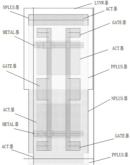
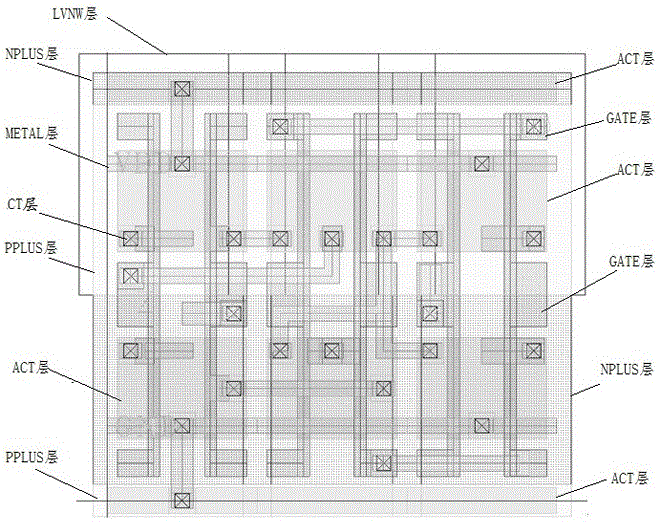
[0045] Such as figure 1 , the structure of the basic unit provided in the present invention. The basic unit of the present invention at least includes GATE layer, ACT layer, LVNW layer, NPULS layer and PPLUS layer, CT layer and METAL layer, all of which have regular shapes. The regular shapes of the GATE layer, the ACT layer, the LVNW layer, the NPULS layer and the PPLUS layer must conform to the process design rules. The process design rules include channel length, number of metal layers, layout size, metal wiring width, spacing and direction, power / ground bus width, and the like.

[0046]The specific regular shape design is: the GATE layer, ACT layer, LVNW layer, NPULS layer and PPLUS layer in the basic unit are symmetrically distributed with the center line in the height direction of the basic unit as the boundary, and / or the center line in the width dir...


PUM


Abstract

The invention discloses a basic cell, standard cell, standard cell library and back-end full-custom design method and a chip manufactured based on the method, and belongs to the technical field of integrated circuit layout designs. The basic cell disclosed by the invention at least comprises GATE layers, ACT layers, an LVNW layer, NPULS layers and PPLUS layers as well as a CT layer and a METAL layer which are all in regular shapes; the regular shapes of the GATE layers, the ACT layers, the LVNW layer, the NPULS layers and the PPLUS layers all need to meet process design rules. The layout of the standard cell comprises M basic cells in different Metal wiring manners, and M is a nonzero integer. The standard cell library comprises a plurality of the standard cells with different functions. The back-end full-custom design method of the invention comprises the following steps: determining the standard cell library, designing the chip based on the standard cell, carrying out analog simulation on a module layout and outputting the layout. The chip realized by adopting the back-end full-custom layout design method is more regular and standard in design to greatly optimize the layout design and improve the layout and processing efficiency so as to shorten the product time to market.

Description

technical field [0001] The invention relates to the technical field of integrated circuit layout design, in particular to a basic unit, a standard unit, a standard unit library, a back-end fully customized design method and a chip realized by the method. Background technique [0002] Integrated circuit layout design includes design based on standard cell library. The design of the standard cell library refers to the design of some standard cells (such as combinational logic, sequential logic, physical cells, etc.) When designing the circuit, call the required standard cells from the standard cell library according to the circuit requirements, and carry out logic synthesis and automatic layout and routing. [0003] The layout design of the standard cell library in the prior art only determines the basic parameters of the layout design according to the relevant process parameters and the technical indicators of the cell library, such as the cell height, line width, wiring cha...

Claims


Application Information

Patent Timeline
Patent Type & Authority Applications(China)
IPC IPC(8): G06F17/50
CPCG06F30/392G06F2115/06
Inventor 王庆霞严斌
Owner HANGZHOU CHIPJET TECH
Why Eureka
Try Eureka