Laminated ceramic electronic component and method for manufacturing same

A technology for electronic components and stacking directions, which is applied in the direction of capacitor manufacturing, fixed capacitance parts, electrical components, etc. Achieves strong fixing force and good joint performance without problems such as poor joint performance

Active Publication Date: 2017-01-25
MURATA MFG CO LTD
View PDF6 Cites 13 Cited by
  • Summary
  • Abstract
  • Description
  • Claims
  • Application Information

AI Technical Summary

Problems solved by technology

In the case of a ceramic electronic component such as a laminated ceramic capacitor in which the internal electrode layer inside the laminate is electrically connected to the external electrode formed on the end face of the laminate, generally, as miniaturization progresses, the internal electrode layer and the extern

Method used


Image

  • Laminated ceramic electronic component and method for manufacturing same
  • Laminated ceramic electronic component and method for manufacturing same
  • Laminated ceramic electronic component and method for manufacturing same

Examples


experiment example 1

[0071] Using the above-mentioned manufacturing method, a multilayer ceramic capacitor was produced. Here, 30 laminated ceramic capacitors with four patterns were fabricated as examples 1 to 4, with the average length of Cu crystals included in the external electrodes expected to be 0.3 μm to 3 μm. In addition, the average length of Cu crystals contained in 30 external electrodes was prepared as a multilayer ceramic capacitor with a desired value of 5 μm, and the average length of Cu crystals contained in the external electrodes was set as a multilayer ceramic capacitor with a desired value of 0.1 μm. 2 kinds of patterns, and as comparative example 1 and comparative example 2. The evaluation of the connectivity with the internal electrode layer is as follows: 30 electrostatic capacitances were measured, and the CV value of the electrostatic capacitance was calculated. If the CV value was 5% or more, the connectivity was evaluated as NG, and when the value was less than 5%, the ...

experiment example 2

[0075] Using the above-mentioned manufacturing method, a multilayer ceramic capacitor was produced, and other evaluations were performed. Here, the number of glasses contained in the external electrodes in contact with the laminate and the number of Cu crystals contained in the external electrodes in contact with the laminate were respectively produced as a pattern with a desired value of 5 or more and a pattern with a desired value of less than 5. . After production, the connectivity with the internal electrode layer and the fixability between the laminate and the external electrodes were evaluated. The evaluation of the connectivity of the internal electrode layers was the same evaluation as in Experimental Example 1. The fixability to the external electrodes was evaluated as follows. On the substrate, a solder made by Senju Metal Industry Co., Ltd. with a trade name of SAC305 was printed with a thickness of 20 μm. Next, the multilayer ceramic capacitor was mounted on the...


PUM

PropertyMeasurementUnit
Sizeaaaaaaaaaa
Sizeaaaaaaaaaa
Average lengthaaaaaaaaaa

Abstract

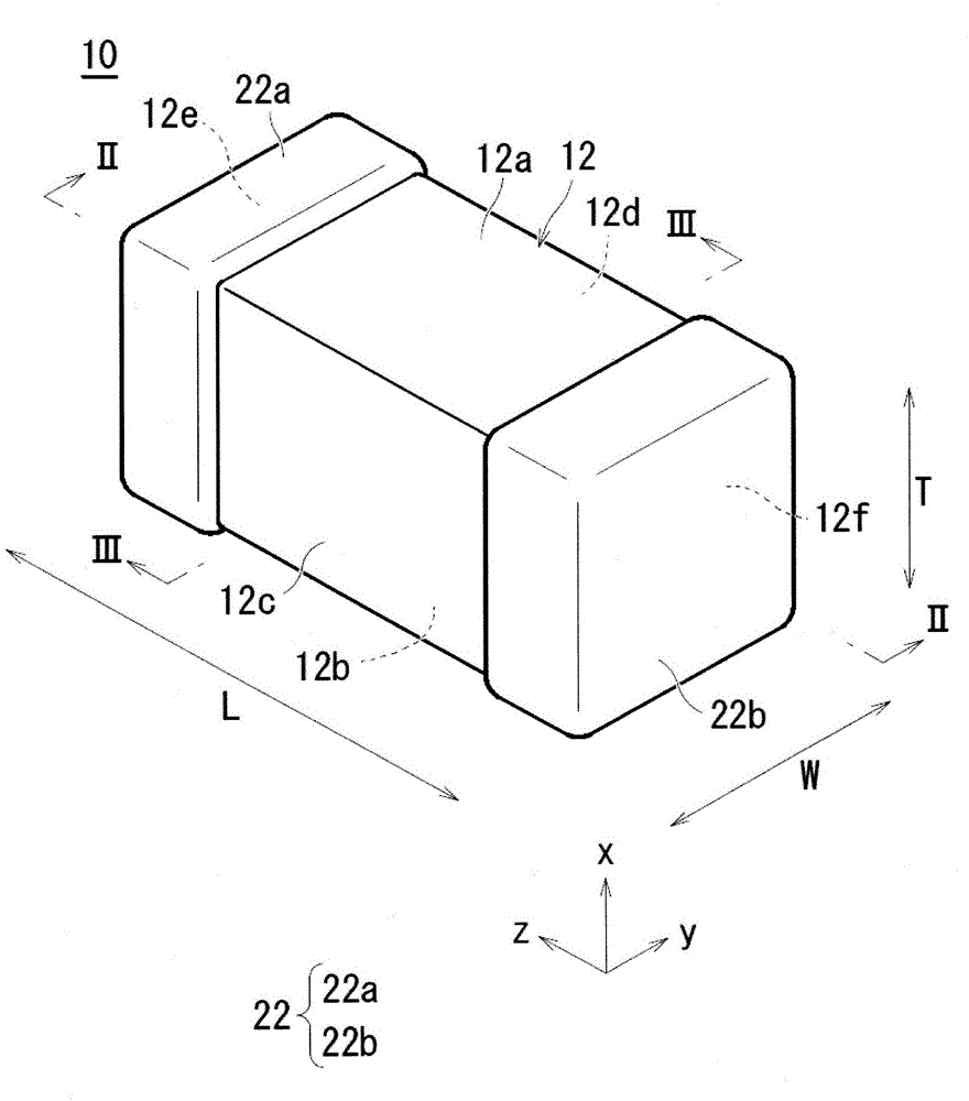
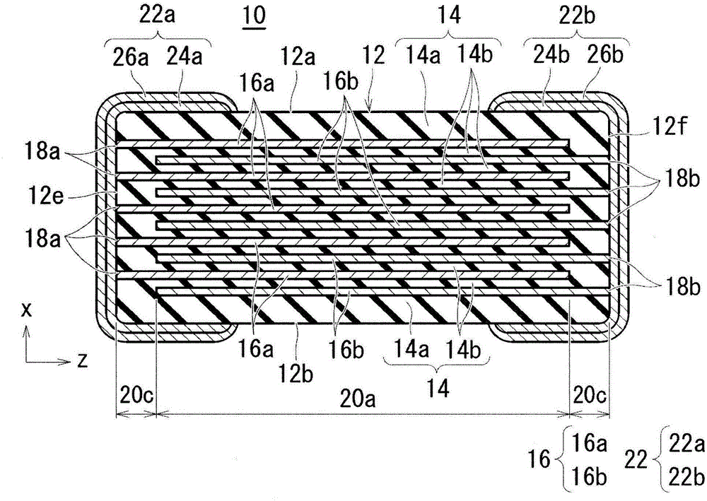
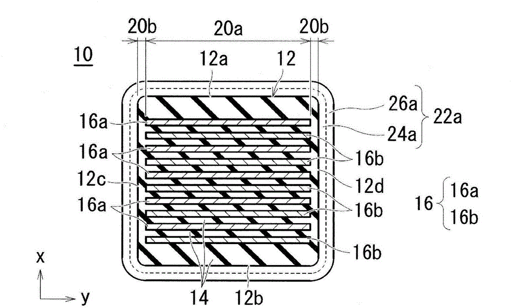
The present invention provides a laminated ceramic electronic component in which the internal electrode layer inside the layered product is bonded to the external electrode and is capable of ensuring a strong fixing force between the external electrode and the stacked body. The laminated ceramic electronic component includes a rectangular parallelepiped laminate (12) in which a plurality of dielectric layers (14) and a plurality of internal electrode layers (16) are laminated, and a laminated body (12) is formed on both end faces of the stacked body (12) (22a, 22b) of the plating layer (26a, 24b) and the coating (26a, 26b). In the case where the cross section including the base electrode layers (24a, 24b) is observed by the FIB SIM image (concentrated ion beam scanning ion microscope), a plurality of Cu crystals and glass, crystal elements having different crystal orientations The average value of the length is 3 [miu] or less.

Description

technical field [0001] The present invention relates to a laminated ceramic electronic component and a method for manufacturing the same, and more particularly, to a laminated ceramic electronic component such as a laminated ceramic capacitor including a laminated body having a plurality of stacked dielectric layers and an external electrode, and a method for manufacturing the same and a plurality of internal electrode layers formed on end faces of the laminate so as to be electrically connected to the internal electrode layers. Background technique [0002] As a small multilayer ceramic electronic component, there are, for example, multilayer ceramic capacitors and the like. A multilayer ceramic capacitor includes a body in which dielectric layers and internal electrode layers are alternately stacked. The internal electrode layers are formed such that a pair of internal electrode layers are alternately exposed from both end surfaces of the body. One of the alternately lam...

Claims


Application Information

Patent Timeline
IPC IPC(8): H01G4/12H01G4/30H01G4/005H01G13/00
CPCH01G4/30H01G4/12H01G4/232H01G4/2325H01G4/005H01G13/00
Inventor 西坂康弘木村真人
Owner MURATA MFG CO LTD
Why Eureka
Try Eureka