Performance test system for low-illumination CMOS chip

A technology for testing system and chip performance, applied in electronic circuit testing, non-contact circuit testing, electrical measurement, etc., can solve the problems of large error and cumbersome operation, and achieve the effect of increasing error, stability and repeatability

Inactive Publication Date: 2017-02-15
NANJING UNIV OF SCI & TECH
View PDF4 Cites 12 Cited by
  • Summary
  • Abstract
  • Description
  • Claims
  • Application Information

AI Technical Summary

Problems solved by technology

Invention patent 201510732802.6 discloses a low-illuminance CMOS signal-to-noise ratio test device, which can only be used to test the signal-to

Method used


Image

  • Performance test system for low-illumination CMOS chip

Examples


Embodiment Construction

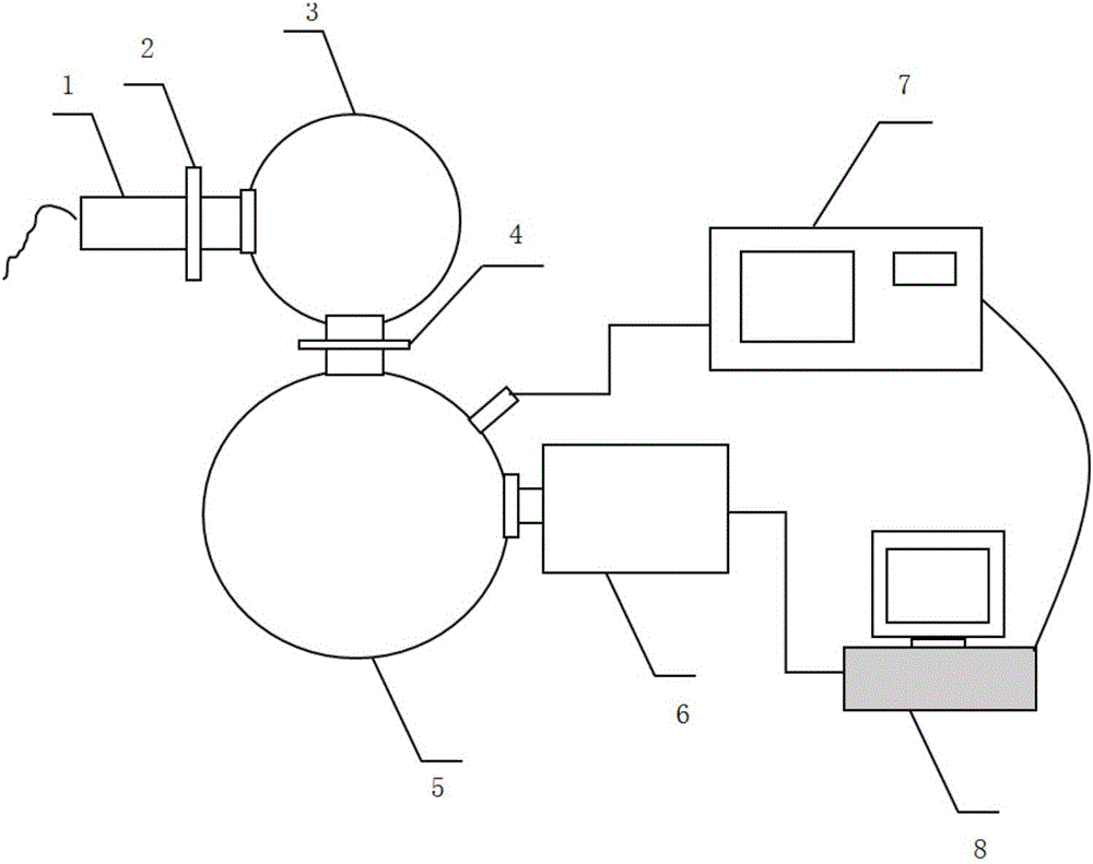
[0012] combine figure 1 , a low-illuminance CMOS chip performance testing system of the present invention, comprising a tungsten-halogen light source 1, an electric slit 2, a first integrating sphere 3, a variable aperture stop 4, a second integrating sphere 5, a dark box 6, and Low illumination CMOS chip, light meter 7 and computer 8;

[0013] The electric slit 2 is arranged between the tungsten halogen light source 1 and the light incident surface of the first integrating sphere 3, and the variable aperture stop 4 is arranged between the light exit surface of the first integrating sphere 3 and the light incident surface of the second integrating sphere 5 Between the surfaces, the light-emitting surface of the second integrating sphere 5 is connected to the entrance of the obscura 6, and the low-illuminance CMOS chip to be tested is built in the obscura 6, and the output end of the low-illuminance CMOS chip is connected to the computer 8. Two apertures are used to connect si...


PUM


Abstract

The invention discloses a performance test system for a low-illumination CMOS chip. The system comprises a halogen tungsten lamp light source, an electric slit, a first integrating sphere, an aperture-variable diaphragm, a second integrating sphere, a camera obscura, the low-illumination CMOS chip to be tested, an illumination meter and a computer, the low-illumination CMOS chip is arranged in the camera obscura, uniform light generated by a halogen tungsten lamp is input to a photosensitive surface of the low-illumination CMOS chip, the computer adjusts the electric slit and the aperture-variable diaphragm to change the illumination, exposure time of the chip is set, an image signal generated by the low-illumination CMOS chip is collected and converted into a corresponding voltage signal, and corresponding parameter values are obtained via data processing. The system can evaluate the performance of the low-illumination CMOS chip scientifically, and provides basis for research and production of low-illumination CMOS.

Description

technical field [0001] The invention belongs to the technical field of low-light testing, in particular to a low-illuminance CMOS chip performance testing system. Background technique [0002] The main parameters of low-illumination CMOS chip performance testing are signal-to-noise ratio, dynamic range, defective pixels, electronic voltage conversion gain, dark current, saturated output current, full well charge, readout noise, responsivity, uniformity, etc., CMOS devices It has the advantages of strong space radiation resistance, large dynamic range, fast readout speed, low cost, small size, light weight, high integration, and low power consumption. It can realize day and night observation, digital transmission, and storage functions, and is widely used in vehicles. / Helmet-mounted image fusion system, gun sight system, laser guidance, security monitoring and many other fields have gradually become the main solid-state imaging devices, so the test of low-light CMOS devices ...

Claims


Application Information

Patent Timeline
IPC IPC(8): G01R31/308G01R31/28
CPCG01R31/2825G01R31/308
Inventor 钱芸生叶琼郭一亮朱波王琦林宇轩徐华
Owner NANJING UNIV OF SCI & TECH
Why Eureka
Try Eureka