Array substrate, manufacturing method thereof and LCD (Liquid Crystal Display)

An array substrate and pixel array technology, which is applied in the field of VA liquid crystal display and liquid crystal display, can solve the problems of insufficient display LCMargin, poor picture display effect, insufficient elastic compression, etc., so as to avoid the loss of transmittance, improve competitiveness, The effect of increasing the contrast

Inactive Publication Date: 2017-02-15
TCL CHINA STAR OPTOELECTRONICS TECH CO LTD
View PDF7 Cites 5 Cited by
  • Summary
  • Abstract
  • Description
  • Claims
  • Application Information

AI Technical Summary

Problems solved by technology

[0003] Assuming that the main spacer (Main CS) and sub-spacer (Sub CS) are designed on the Gate line, if the cell thickness of the LCD panel is 3.5um, the height occupied by the R / B color resist stack is deducted at this time , the height of the designed Main CS is only 0.8um, which leads to insufficient elastic compression of CS
In the end, the display of LC Margin is not enough, which affects the product yield
In addition, since the Gate line and the Data line are located at the R / B color-resist stacked place, the flatness of the terrain is poor, resulting in poor picture display effect and prone to uneven brightness. In order to improve the above-mentioned defects, it has to be selected PFA is used as a flat layer, which increases the cost of the product

Method used


Image

  • Array substrate, manufacturing method thereof and LCD (Liquid Crystal Display)
  • Array substrate, manufacturing method thereof and LCD (Liquid Crystal Display)
  • Array substrate, manufacturing method thereof and LCD (Liquid Crystal Display)

Examples


Embodiment Construction

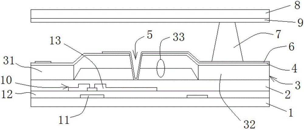
[0031] The following will describe in detail with reference to the accompanying drawings, the array substrate and its manufacturing method, and the liquid crystal display of the present invention.

[0032] combine figure 1 , the array substrate proposed by the present invention will be described in detail.

[0033] The array substrate proposed by the present invention, from bottom to top, is a glass substrate 1 containing a thin film transistor array, a first passivation layer 2, a red, green and blue pixel array layer 3, a second passivation layer 4, via holes 5, a second passivation layer A transparent conductive layer 6 , in the red, green and blue pixel array layer 3 , red and blue resist stacks 33 are arranged between pixels.

[0034] The thin film transistor includes a first metal layer 11, a gate insulating layer 12, an active layer, an ohmic contact layer, and a second metal layer 13 from bottom to top, and the first metal layer includes a gate electrode and an electr...


PUM


Abstract

The invention discloses a colored film array substrate in the field of VA (Vertical Alignment) display. The colored film array substrate comprises an RGB (Red, Green and Blue) pixel array layer, wherein a red and blue color resistance stack is arranged between pixels in the RGB pixel array layer, a certain quantity of black cushion spacers are arranged above the pixels, a whole liquid crystal panel is supported by the black cushion spacers, meanwhile, a shading function is obtained as the black cushion spacers are used as a frame, the black cushion spacers are arranged above the pixels which are relatively flat, and a PFA (Polyfluoroalkoxy) material serving as a flat layer is not needed, so that the cost is reduced. The invention also provides an LCD (Liquid Crystal Display) comprising the colored film array substrate. The LCD comprises the colored film array substrate and an upper substrate. Since black matrixes on the colored film array substrate are eliminated and the black cushion spacers are arranged on the colored film array substrate, penetration rate loss caused by poor alignment accuracy during an alignment process of the colored film array substrate and the upper substrate is avoided. The invention further provides a manufacturing method of the colored film array substrate.

Description

technical field [0001] The invention relates to the field of VA liquid crystal displays, in particular to a substrate, a manufacturing method thereof, and a liquid crystal display. Background technique [0002] For the in-plane switching display mode, since the arrangement of the liquid crystal is driven by a horizontal electric field, the flatness of the plane where the electrode is located is very high, so in addition to the RGB color photoresist, a layer of color photoresist is generally covered Transparent photoresist to improve planarity. Therefore, the BM-Less technology developed on the basis of the IPS display mode can use red and blue photoresist stacks on both the data line (DataLine) and the gate line (Gate Line) to achieve light shading. This technology has been realized by the company Mass production. However, for the VA (Vertical Alignment) display mode, the flat layer is generally not covered due to cost considerations. When developing BM-less technology, i...

Claims


Application Information

Patent Timeline
IPC IPC(8): G02F1/1362G02F1/1339H01L27/12H01L21/77
CPCG02F1/136209G02F1/13394G02F1/136213G02F1/136227H01L27/1214H01L27/1259
Inventor 于承忠
Owner TCL CHINA STAR OPTOELECTRONICS TECH CO LTD
Why Eureka
Try Eureka