Graphene/gallium arsenide solar cell preparation method

A solar cell and gallium arsenide technology, applied in the field of solar energy, can solve the problems of only 3.36% efficiency and unsatisfactory effect, and achieve the effects of facilitating industrial application, improving photoelectric conversion efficiency, and increasing fill factor

Active Publication Date: 2017-02-15
INST OF MICROELECTRONICS CHINESE ACAD OF SCI
View PDF5 Cites 2 Cited by
  • Summary
  • Abstract
  • Description
  • Claims
  • Application Information

AI Technical Summary

Problems solved by technology

Some researchers also combine graphene with gallium arsenide materials to form Schottky junction solar cells, but the efficiency is only 3.36%, and the effect is far from ideal.

Method used


Image

  • Graphene/gallium arsenide solar cell preparation method
  • Graphene/gallium arsenide solar cell preparation method
  • Graphene/gallium arsenide solar cell preparation method

Examples


preparation example Construction

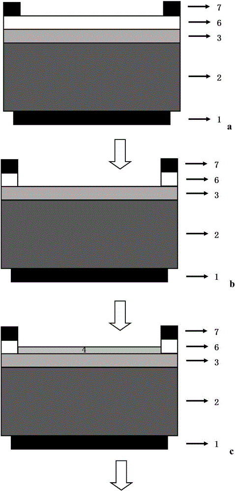
[0024] The invention provides a method for preparing a graphene / gallium arsenide solar cell, comprising the following steps:

[0025] 1) Prepare a window layer on the surface of the gallium arsenide epitaxial wafer, and then prepare a heavily doped gallium arsenide cap layer on the surface of the window layer;

[0026] 2) preparing a front electrode on the surface of the heavily doped gallium arsenide cap layer, and preparing a back electrode on the surface of the gallium arsenide epitaxial wafer away from the window layer;

[0027] 3) The heavily doped gallium arsenide cap layer between the front electrode grid lines is etched by a chemical etching method to expose the window layer;

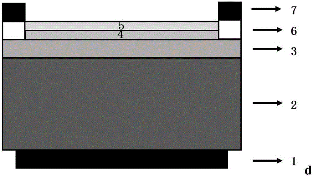
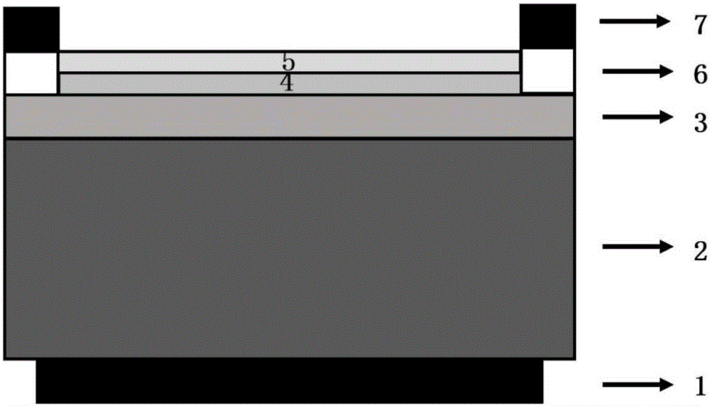
[0028] 4) preparing a graphene layer on the surface of the exposed window layer;

[0029] 5) preparing an anti-reflection layer on the surface of the graphene layer to obtain the graphene / gallium arsenide solar cell.

[0030] In the present invention, gallium arsenide epitaxial wafers are firs...

Embodiment 1

[0082] 1) Epitaxial growth of 0.5 μm thick n-type GaAs buffer layer, 0.1 μm thick n-type AlGaAs back field, 3.2 μm thick n-type GaAs base layer, 0.5 μm thick p-type GaAs emitter layer on n-type GaAs substrate by MOCVD method, Then continue to epitaxially grow the p-type AlGaAs window layer with a thickness of 0.03 μm and the p-type heavily doped GaAs cap layer with a thickness of 0.5 μm;

[0083] 2) The n-type electrode of NiGeAu system is evaporated by electron beam on the lower surface as the back electrode, and the p-type electrode of TiPdAg system is evaporated by electron beam on the cap layer on the upper surface as the front electrode.

[0084] 3) Soak the epitaxial wafer in acetone at 60°C for half an hour, then rinse it with isopropanol, ethanol and deionized water; prepare a solution with a ratio of hydrochloric acid to water of 1:1, soak the epitaxial wafer for two minutes and then rinse it; Cover the hat layer pattern to be protected on the upper surface with photo...

Embodiment 2

[0095] 1) Epitaxial growth of 0.5 μm thick n-type GaAs buffer layer, 0.1 μm thick n-type AlGaAs back field, 3.2 μm thick n-type GaAs base layer, 0.5 μm thick p-type GaAs emitter layer on n-type Ge substrate by MOCVD method, Then continue to epitaxially grow the p-type AlGaAs window layer with a thickness of 0.03 μm and the p-type heavily doped GaAs cap layer with a thickness of 0.5 μm;

[0096] 2) The n-type electrode of NiGeAu system is evaporated by electron beam on the lower surface as the back electrode, and the p-type electrode of TiPdAg system is evaporated by electron beam on the cap layer on the upper surface as the front electrode.

[0097]3) Thin the epitaxial wafer substrate to the required thickness, soak it in acetone at 60°C for half an hour, then rinse it with isopropanol, ethanol and deionized water, and dry it with nitrogen; prepare piranha lotion and soak the epitaxial wafer Thirty seconds later, rinse it off and dry it with nitrogen; cover the cap layer to b...


PUM


Abstract

The invention provides a graphene / gallium arsenide solar cell preparation method. The graphene / gallium arsenide solar cell preparation method comprises the following steps of: 1) preparing a window layer on the surface of a gallium arsenide epitaxial wafer and then preparing a heavily-doped gallium arsenide cap layer on the surface of the window layer; 2) preparing a positive electrode on the surface of the heavily-doped gallium arsenide cap layer, and preparing a negative electrode on the surface of the gallium arsenide epitaxial wafer away from the window layer; 3) etching the heavily-doped gallium arsenide cap layer between positive electrode grid lines by the chemical etching method so as to expose the window layer; 4) preparing a graphene layer on the surface of the exposed window layer; 5) preparing an anti-reflection layer on the surface of the graphene layer to obtain a graphene / gallium arsenide solar cell. In the invention, graphene is applied to the gallium arsenide solar cell as a transparent conductive material, so the conversion efficiency of the gallium arsenide solar cells is further improved and is much higher than that of graphene / gallium arsenide Schottky junction solar cells. In addition, the cost for solar cell preparation is low and the process is simple, which is conducive to industrialization application.

Description

technical field [0001] The invention relates to the technical field of solar energy, in particular to a preparation method of a graphene / gallium arsenide solar cell. Background technique [0002] As the source of life on earth, solar energy has always been the first choice among new energy sources. The solar power reaching the earth is extremely huge, up to 173,000TW, which is equivalent to providing the energy contained in 5 million tons of coal per second. Solar cells that can directly convert solar energy into electricity have become the focus of attention. Among the current photovoltaic power generation technologies, silicon-based solar cells, especially crystalline silicon solar cells, still occupy a major market share. However, the pollution problem caused by the purification process of silicon materials and its complicated preparation process also make the development of silicon solar cells encounter bottlenecks. Compared with silicon materials, gallium arsenide ha...

Claims


Application Information

Patent Timeline
IPC IPC(8): H01L31/18H01L31/0224H01L31/0216
CPCH01L31/02168H01L31/022425H01L31/184Y02E10/544Y02P70/50
Inventor 孙恒超贾锐陶科戴小宛金智刘新宇
Owner INST OF MICROELECTRONICS CHINESE ACAD OF SCI
Why Eureka
Try Eureka