
Method for producing waveguide substrate

A manufacturing method and substrate technology, which are applied in the directions of waveguide, semiconductor/solid-state device manufacturing, and waveguide-type devices, etc., can solve the problems of metal film peeling, difficult to reach plating solution, and inability to ensure metal film, and achieve the effect of preventing peeling.

Inactive Publication Date: 2017-02-15
FUJIKURA LTD
View PDF2 Cites 4 Cited by
  • Summary
  • Abstract
  • Description
  • Claims
  • Application Information

AI Technical Summary

Problems solved by technology

[0006] However, when the non-through hole forming the conductor pin has a small diameter and a high aspect ratio, for example, the hole diameter is 100 μm or less, and the depth is about 460 μm, it is difficult for the plating solution to reach the bottom surface of the non-through hole, so a sufficient coating cannot be ensured near the bottom surface. Impedance matching is not possible due to thick metal film
[0007] In addition, if the metal film thickness is ensured only by sputtering near the bottom surface of the non-through hole without plating, the film thickness of the metal film for ground conductor formed on the surface of the substrate becomes thicker than necessary. There is a problem that the metal film is easily peeled off from the substrate due to the difference in expansion coefficient between the metal film and the substrate

Method used


Image

  • Method for producing waveguide substrate
  • Method for producing waveguide substrate
  • Method for producing waveguide substrate

Examples


Embodiment Construction

[0019] [Structure of waveguide substrate]

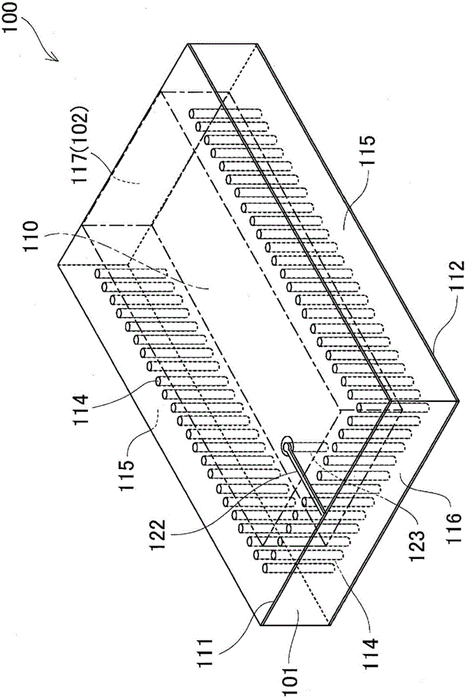
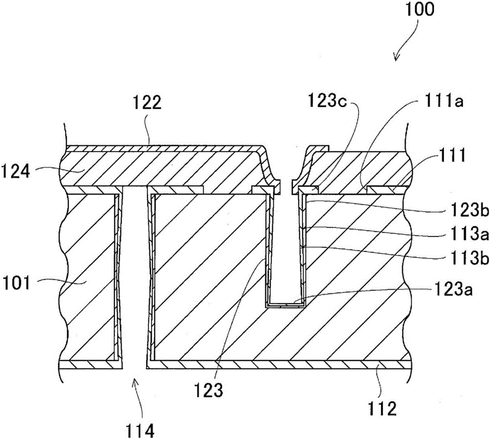
[0020] figure 1 is a perspective view showing the waveguide substrate 100, figure 2 is an end view showing the waveguide substrate 100 . It should be noted that although the conductor column 114 and the transmission path 122 are as figure 1 not present on the same face as shown, but on figure 2 Both are shown in the same end view for ease of presentation.

[0021] Such as figure 1 as well as figure 2 As shown, the waveguide substrate 100 of this embodiment includes: a glass substrate 101, a transmission path (planar circuit) 122 for signal propagation, a conductor pin 123, and a first ground conductor layer 111 and a second ground conductor layer 112 connected to a ground potential. , and waveguide 110 .

[0022] The glass substrate 101 is a glass substrate made of a single material. Instead of the glass substrate, a quartz substrate or a semiconductor substrate may be used.

[0023] The waveguide 110 is composed of a fir...


PUM


Abstract

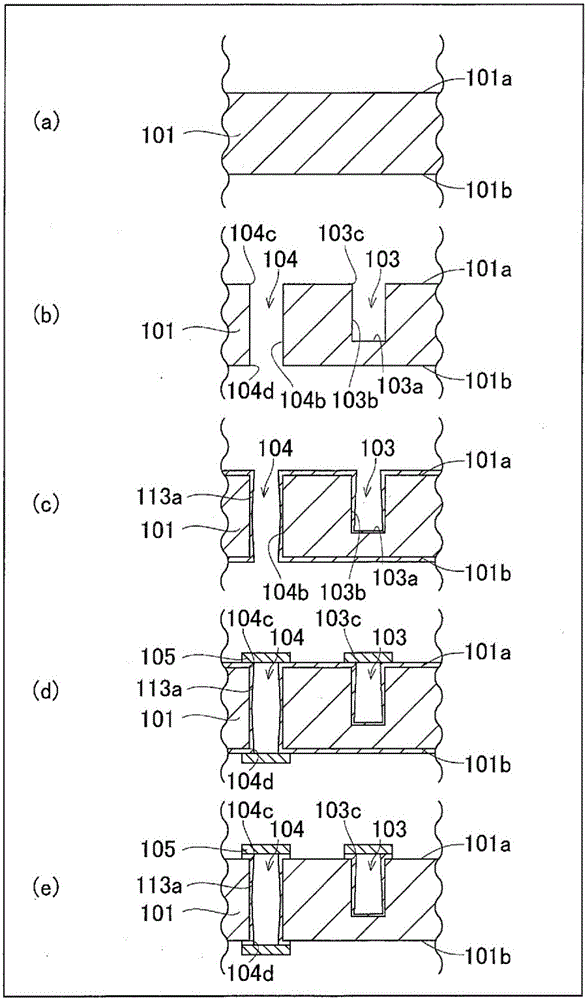
To allow a metal film to have a sufficient thickness around a bottom surface of a non-through hole and prevent the metal film from being peeled from a substrate surface, a method for producing a waveguide substrate includes forming a first metal film on (i) a first main surface of a substrate, at which first main surface a non-through hole opens, and on (ii) an inner wall of the non-through hole, forming resist on a first main surface side of the substrate in such a manner that the resist blocks the opening of the non-through hole, removing a first portion of the first metal film which first portion is on the first main surface, removing the resist, and forming a second metal film on the first main surface of the substrate in a state where the first metal film is present on the inner wall of the non-through hole.

Description

technical field [0001] The present invention relates to a method of manufacturing a waveguide substrate. Background technique [0002] A millimeter-wave communication module using a post-wall waveguide (hereinafter sometimes referred to as “PWW”) is known as a method for realizing an inexpensive and small millimeter-wave communication module (for example, refer to Patent Document 1). [0003] This PWW is a waveguide as follows: a printed circuit board with a ground conductor formed on the surface and the back surface, and a plurality of column walls that stand up between the ground conductor layers, that is, conductor columns, are arranged. The conductor columns are equivalent to conventional waveguides. metal side walls. In the above-mentioned millimeter wave communication module, the wireless communication IC mounted on the substrate of the PWW is connected to the transmission line (microstrip line, coplanar line, strip line, etc.) by wire bonding, bump connection, etc. ...

Claims


Application Information

Patent Timeline
IPC IPC(8): H01P11/00H01P3/00
CPCH01P3/00H01P11/001H01L21/4846H01P3/121H01P5/107H01L23/49827H01L23/66G02B6/00
Inventor 韩旭
Owner FUJIKURA LTD
Learn More