Check patentability & draft patents in minutes with Patsnap Eureka AI!

A charge probe based on a single-electron transistor and its preparation method

A technology of single-electron transistors and probes, which is applied in the direction of manipulating single atoms, processes for producing decorative surface effects, and nanostructure manufacturing, which can solve the problems of low preparation efficiency and high difficulty

Inactive Publication Date: 2017-11-28
NAT UNIV OF DEFENSE TECH
View PDF7 Cites 0 Cited by
  • Summary
  • Abstract
  • Description
  • Claims
  • Application Information

AI Technical Summary

Problems solved by technology

[0003] Due to the difficulty of preparing SET technology on fiber optic probes and the low preparation efficiency, based on the above-mentioned SET probe technology and in view of its shortcomings, people have improved and optimized the SET probe technology.

Method used


Image

  • A charge probe based on a single-electron transistor and its preparation method
  • A charge probe based on a single-electron transistor and its preparation method
  • A charge probe based on a single-electron transistor and its preparation method

Examples


preparation example Construction

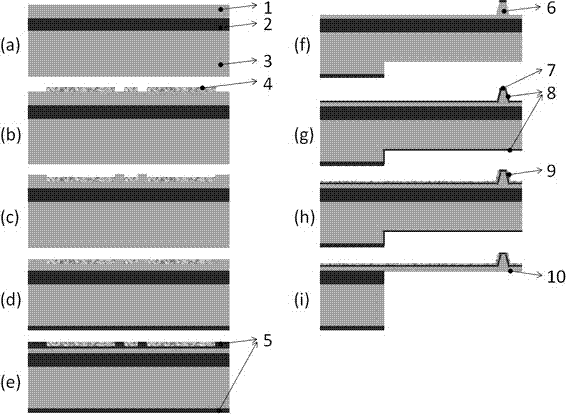
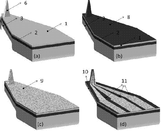
[0045] A preparation method of a SET-based charge probe, comprising the steps of:

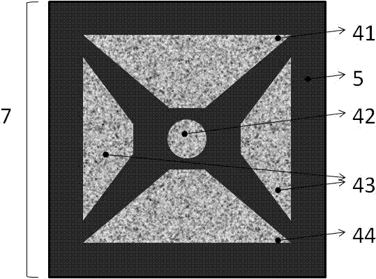
[0046] (1) Using SOI as the substrate, prepare the source, drain, side gate, barrier layer and Coulomb island basic structure of the SET on the top silicon of the SOI substrate;

[0047] (2) Etching the top layer of silicon by metal-assisted chemical etching to a certain depth;

[0048] (3) Remove a certain thickness of the top layer of silicon by grinding, and then oxidize the SOI substrate, so that the source, drain, side gate and Coulomb island of the SET are embedded in the silicon dioxide to form a tunneling barrier , and then use plasma enhanced chemical vapor deposition (PECVD) to deposit a certain thickness of silicon dioxide as a protective layer;

[0049] (4) The needle tip of the probe is prepared by ultraviolet lithography and wet etching process;

[0050] (5) Using oxidation, magnetron sputtering, focused ion beam (FIB) etching and focused ion beam induced deposition processes to...


PUM

PropertyMeasurementUnit
thicknessaaaaaaaaaa
thicknessaaaaaaaaaa
thicknessaaaaaaaaaa

Abstract

The invention relates to a charge probe based on a single electron transistor (SET) and a preparation method thereof. The SET is integrated on the head face of a pinpoint of a probe cantilever beam; the source, the drain, the side grid and the coulomb island of the SET are embedded in silicon dioxide on the head face of the pinpoint of the probe cantilever beam; the charge probe takes a silicon-on-insulator (SOI) as a substrate; basic composition units of the SET are the source, the drain, the side grid, the coulomb island and a tunnel barrier integrated on the top silicon of the substrate; furthermore, the SET is positioned on the head face of the charge probe pinpoint, wherein gold nanoparticles are used as the coulomb island of the SET, and positioned among the source, the drain and the side grid; the coulomb island is encircled by a silicon dioxide medium obtained by oxidization of the top silicon of the substrate; the coulomb island, the source and the drain are coupled in a tunnel combination manner; and the coulomb island and the side grid are coupled in a capacitance manner. By means of the charge probe based on the SET and the preparation method thereof disclosed by the invention, a foundation is established for performing high-sensitivity scanning detection of sample surface charge distribution at the nanoscale level by an atomic power SET scanning probe.

Description

technical field [0001] The invention relates to the field of nanoelectronic devices and micro-nano sensors, in particular to a charge probe based on a single-electron transistor and a preparation method thereof, which are used for charge scanning detection. Background technique [0002] Quantum dot single-electron transistors (SETs) based on the Coulomb blocking effect and electron tunneling effect have extremely high sensitivity to small charge changes in their adjacent areas, and are suitable for fixed-point high-sensitivity charge detection at the micro-nano scale. The core of SET sensitive to charge is the Coulomb island with a scale of only tens of nanometers. The source and drain electrodes are coupled to the Coulomb island through the tunneling barrier, and the control gate and the Coulomb island are coupled through capacitive coupling. SET is suitable for fixed-point high-sensitivity charge detection at the micro-nano scale. With the development and maturity of nano...

Claims


Application Information

Patent Timeline
Patent Type & Authority Patents(China)
IPC IPC(8): B81C1/00B82B1/00B82B3/00
CPCB81C1/00015B81C1/00111B82B1/00B82B3/00B82B3/0009
Inventor 方靖岳李欣幸王飞张学骜秦华常胜利秦石乔
Owner NAT UNIV OF DEFENSE TECH
Features
  • R&D
  • Intellectual Property
  • Life Sciences
  • Materials
  • Tech Scout
  • Unparalleled Data Quality
  • Higher Quality Content
  • 60% Fewer Hallucinations
Learn More