Graphene electroluminescence dot matrix display panel and manufacturing method thereof
A technology of dot matrix display and production method, applied in the field of graphene electroluminescence dot matrix display panel and its production, can solve the problems of easy damage of electroluminescence cold light sheet, poor light transmittance, high price, etc., and achieve excellent Electricity, simple production process, rich display effect
- Summary
- Abstract
- Description
- Claims
- Application Information
AI Technical Summary
Problems solved by technology
Method used
Image
Examples
Embodiment 1
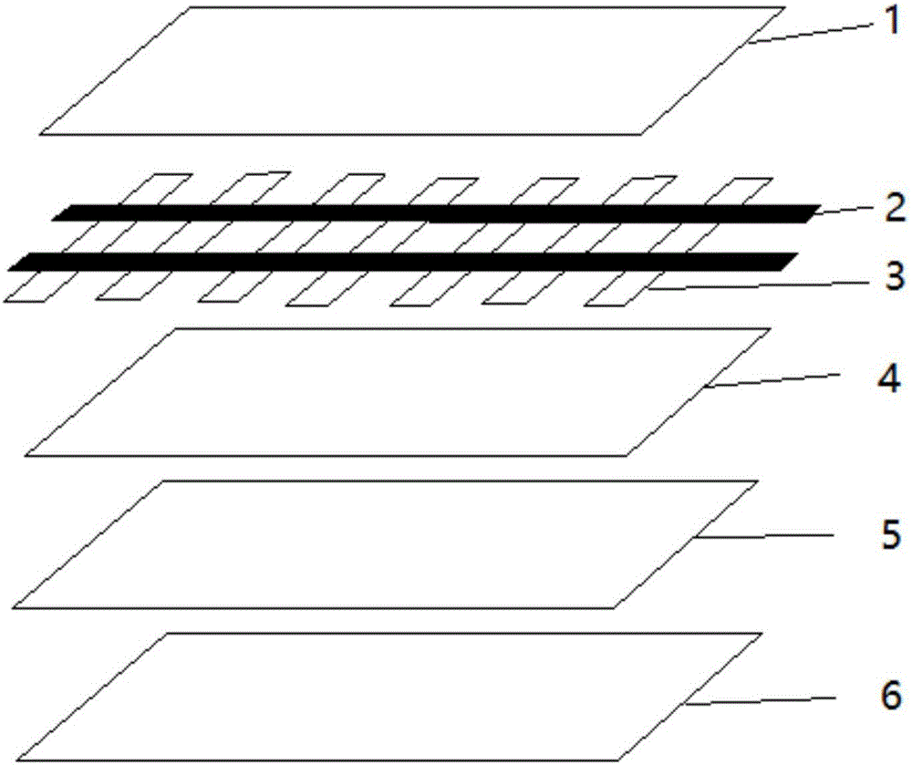
[0042] The graphene electroluminescent matrix display panel manufacturing method of the present embodiment comprises the following steps:
[0043] A. The upper conductive layer 1 is prepared by using a graphene film with impurities removed from the surface, and the graphene film is dried at a temperature of 100° C. for 20 minutes to prepare the upper conductive layer 1 .
[0044] B. Print a luminescent material 2 with a thickness of 1 μm on one of the surfaces of the conductive layer 1 on the graphene film. The luminescent material 2 is printed horizontally and then vertically to form a matrix 3, which is the luminescent layer, and is cured, specifically on the upper surface. After the luminescent material 2 is printed on the surface of the conductive layer 1, it is cured at 110°C for 30 minutes; the luminescent material 2 of this embodiment is ZnS:Mn, and the mass ratio of Mn to ZnS is 1:100, and the luminescent material 2 is prepared as The aqueous solution is used for print...
Embodiment 2
[0051] The graphene electroluminescent matrix display panel manufacturing method of the present embodiment comprises the following steps:
[0052] A. The upper conductive layer 1 is prepared by using a graphene film with impurities removed from the surface, and the graphene film is dried at a temperature of 140° C. for 10 minutes to obtain the upper conductive layer 1 .
[0053] B. Print a luminescent material 2 with a thickness of 20 μm on one of the surfaces of the upper conductive layer 1. The luminescent material 2 is first printed horizontally and then vertically to form a matrix 3, which is the luminescent layer and cured, specifically on the upper conductive layer 1. After printing the luminescent material 2, place it at 130°C for 10 minutes to cure; the luminescent material 2 is selected from one or more combinations of ZnS:Mn, ZnS:Tb, SrS:Ce, the luminescent material 2 of this embodiment SrS:Ce is selected, the mass ratio of Ce to SrS is 0.1:100, and the luminescent m...
PUM
| Property | Measurement | Unit |
|---|---|---|
| thickness | aaaaa | aaaaa |
| thickness | aaaaa | aaaaa |
| thickness | aaaaa | aaaaa |
Abstract
Description
Claims
Application Information
