Semiconductor structure manufacturing method

A manufacturing method and semiconductor technology, which are applied to semiconductor devices, electric solid-state devices, electrical components, etc., can solve the problems of easy occurrence of holes in floating gates and reduced device performance, so as to improve breakdown performance, reduce area, and improve coupling rate. Effect

Active Publication Date: 2017-03-01
SEMICON MFG INT (SHANGHAI) CORP
View PDF5 Cites 13 Cited by
  • Summary
  • Abstract
  • Description
  • Claims
  • Application Information

AI Technical Summary

Problems solved by technology

[0007] In view of the above-mentioned shortcomings of the prior art, the object of the present invention is to provide a method for manufacturing a semiconductor structure, which is used to solve the problem in the prior art that holes are prone to appear in the floating gate, resulting in a decrease in device performance

Method used


Image

  • Semiconductor structure manufacturing method
  • Semiconductor structure manufacturing method
  • Semiconductor structure manufacturing method

Examples


Embodiment 1

[0065] The present invention provides a manufacturing method of a semiconductor structure, please refer to figure 1 , Shown as the process flow chart of the method, including the following steps:

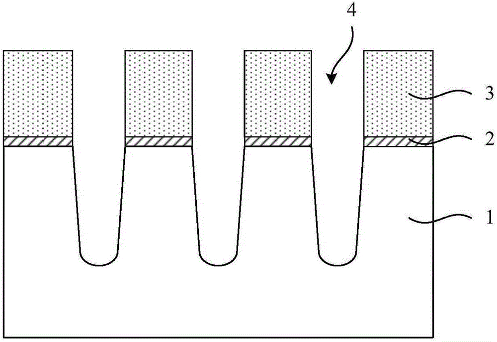
[0066] S1: Provide a substrate, sequentially form a pad oxide layer and a silicon nitride layer on the surface of the substrate, and form at least one recess that penetrates the pad oxide layer and the silicon nitride layer and penetrates into the substrate groove;

[0067] S2: Fill the groove with an insulating dielectric material to form an isolation structure, and perform planarization so that the upper surface of the isolation structure is flush with the upper surface of the silicon nitride layer;

[0068] S3: removing the silicon nitride layer of the first thickness from the top, exposing the first section of the isolation structure, and etching the isolation structure back to reduce the width of the first section of the isolation structure;

[0069] S4: further remove the second thick...

Embodiment 2

[0097] This embodiment adopts basically the same technical solution as the first embodiment, and the difference lies in the shape of the finally formed floating gate structure.

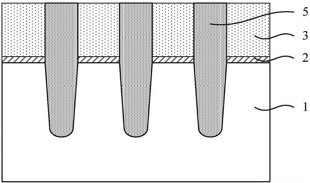
[0098] First, perform steps S1 to S4 that are basically the same as in the first embodiment to obtain Figure 7 The structure shown.

[0099] Then see Figure 15 Step S5 is performed: Step S4 is repeated several times until the silicon nitride layer 3 is etched.

[0100] Specifically, in this step, the number of repeating step S4 is 2-100 times, preferably more than 10 times. The thickness of the silicon nitride layer removed during each repetition of step S4 is the same, or all are different, or at least two different. The thickness of the silicon nitride layer removed during each repetition of step S4 ranges from 1 to 50 angstroms, preferably less than 10 angstroms.

[0101] Each time step S4 is repeated, one more small step is formed. A plurality of small steps are connected in sequence to form the incli...


PUM


Abstract

The invention discloses a semiconductor structure manufacturing method, which comprises the following steps: 1) forming at least one concave groove that penetrates a silicon nitride layer and goes deep into a substrate; 2) forming an isolation structure; 3) removing from the top a first thickness silicon nitride layer so as to expose the first section of the isolation structure; and conducting an etchback to the isolation structure to reduce the width of the first section; 4) further removing a second thickness silicon nitride layer so as to expose the second section of the isolation structure; and conducting an etchback to the isolation structure to reduce the width of the second section; 5) repeating the step 4 at least one time until the remaining silicon nitride layer is provided with a third thickness; 6) removing the remaining silicon nitride layer; and 7) depositing and obtaining a floating gate structure. According to the invention, in the manufacturing process of the floating gate, the floating gate is gradually enlarged to fill the upper opening while the active region CD at the bottom does not have to be enlarged. In this way, it is possible to enlarge the processing window and effectively avoid the appearance of holes in the floating gate. And it is also possible to better regulate the shape and appearance of the floating gate, increase the coupling rate of components and improve the breakdown performance between the active region and the control gate.

Description

Technical field [0001] The invention belongs to the field of semiconductor technology and relates to a method for manufacturing a semiconductor structure. Background technique [0002] In the current semiconductor industry, integrated circuit products can be divided into three main types: logic, memory, and analog circuits. Among them, memory devices account for a large proportion of integrated circuit products, such as RAM (random access memory), DRAM (dynamic Random Access Memory), ROM (Read Only Memory), EPROM (Erasable Programmable Read Only Memory), FLASH (Flash Memory), FRAM (Ferroelectric Memory), etc. The development of flash memory devices in memories has been particularly rapid, and they have become the mainstream of non-volatile semiconductor storage technology. Its main feature is that it can maintain the stored information for a long time without power on. It has many advantages such as high integration, faster access speed and easy erasing, so it is obtained in man...

Claims


Application Information

Patent Timeline
Patent Type & Authority Applications(China)
IPC IPC(8): H01L27/11521
CPCH10B41/00
Inventor 王新鹏
Owner SEMICON MFG INT (SHANGHAI) CORP
Why Eureka
Try Eureka