High-K metal gate structure, fin type field effect transistor and manufacturing methods therefor

A technology of metal gate and fabrication method, which is applied in semiconductor/solid-state device manufacturing, semiconductor devices, electrical components, etc., can solve problems such as transistor performance mismatch and transistor matching performance degradation, and achieve improved matching performance and stable electrical properties. , the effect of preventing the mismatch problem

Active Publication Date: 2017-03-08
SEMICON MFG INT (SHANGHAI) CORP
View PDF4 Cites 6 Cited by
  • Summary
  • Abstract
  • Description
  • Claims
  • Application Information

AI Technical Summary

Problems solved by technology

[0003] However, the high-K metal gate structure made by the existing manufacturing method can easily lead to a decrease in the matching performance of the transistor, that is, the performance mismatch problem of the transistor (Mismatch)

Method used


Image

  • High-K metal gate structure, fin type field effect transistor and manufacturing methods therefor
  • High-K metal gate structure, fin type field effect transistor and manufacturing methods therefor
  • High-K metal gate structure, fin type field effect transistor and manufacturing methods therefor

Examples


Embodiment Construction

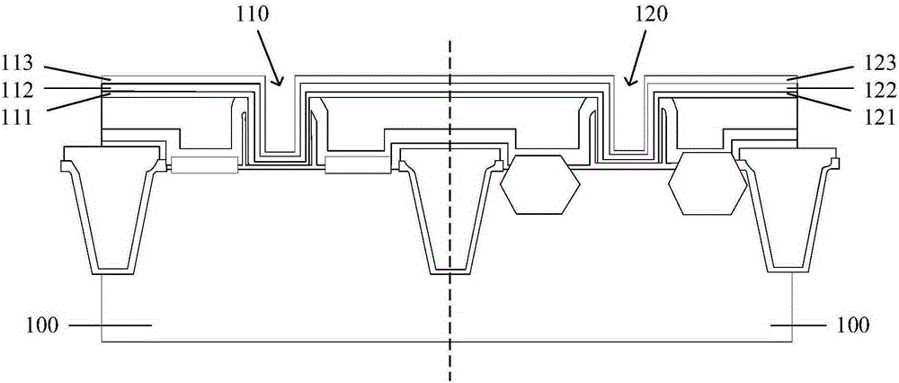
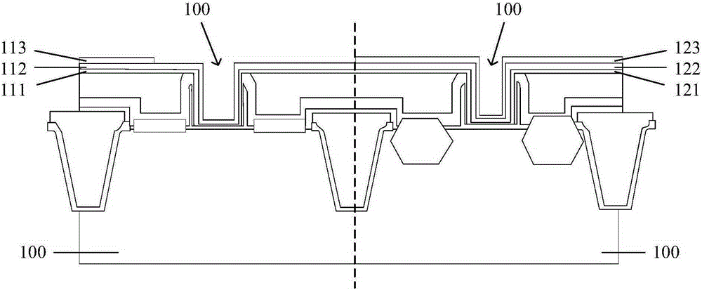
[0034] As mentioned in the background art, the existing manufacturing method easily leads to a decrease in the matching performance of the NMOS transistor and the PMOS transistor. According to the analysis of the inventors, it turns out that in the semiconductor structure using aluminum as the metal gate, the matching performance of transistors (NMOS transistors and PMOS transistors, etc.) is seriously degraded due to the problem of aluminum diffusion; however, for the semiconductor structure using tungsten as the metal gate In the semiconductor structure, although the problem of aluminum diffusion no longer exists, the matching performance of the transistor still decreases. The inventor further analyzed and found that the original tungsten metal gate is formed by chemical vapor deposition (CVD), and when CVD forms a tungsten metal gate, the precursor used is usually tungsten hexafluoride (WF 6 ) or tungsten tetrafluoride (WF 4 ), and the fluorine in tungsten hexafluoride or ...


PUM


Abstract

The invention discloses a high-K metal gate structure, a fin type field effect transistor and manufacturing methods therefor. The manufacturing method for the high-K metal gate structure comprises the steps of providing a semiconductor substrate, and forming a first barrier layer on a first work function metal layer in a first groove; forming a second barrier layer on a second work function metal layer in a second groove; performing first silicon ion implantation on the first barrier layer in the first groove; performing second silicon ion implantation on the second barrier layer in the second groove; after performing first silicon ion implantation on the first barrier layer, filling the first groove with a first tungsten metal gate; after performing second silicon ion implantation on the second barrier layer, filling the second groove with a second tungsten metal gate; and after performing the first silicon ion implantation and the second silicon ion implantation, performing at least one step of thermal treatment. By adoption of the method, the matching performance of the transistor is improved, and the problem of performance mismatch of the transistor can be prevented.

Description

technical field [0001] The invention relates to the field of semiconductor manufacturing, in particular to a high-K metal gate structure, a fin field effect transistor and a manufacturing method thereof. Background technique [0002] In the traditional MOS transistor process, silicon dioxide is usually used as the gate dielectric, and heavily doped polysilicon is used as the gate material. With the development of integration and miniaturization of semiconductor devices, MOS devices using a gate dielectric layer made of silicon dioxide and a gate layer of polysilicon have problems such as increased leakage and gate loss. In order to solve the above problems, the high K (high dielectric constant insulating layer) metal gate (High K Metal Gate, HKMG) process has become a research hotspot, and the fabrication method of the high K metal gate structure is widely used in the current semiconductor process Process. [0003] However, the high-K metal gate structure manufactured by t...

Claims


Application Information

Patent Timeline
IPC IPC(8): H01L21/28H01L29/49H01L21/336
CPCH01L21/28008H01L29/4958H01L29/66795
Inventor 李勇
Owner SEMICON MFG INT (SHANGHAI) CORP
Why Eureka
Try Eureka