Photovoltaic assembly and photovoltaic power generating system
A photovoltaic module and light-receiving surface technology, which is applied in the field of solar cells, can solve the problems of insufficient bonding force between the single-layer anti-reflection film layer and the substrate, low anti-reflection performance of the anti-reflection film layer, and single control means, so as to reduce internal stress , Reduce insulation, good anti-reflection effect
- Summary
- Abstract
- Description
- Claims
- Application Information
AI Technical Summary
Problems solved by technology
Method used
Image
Examples
Embodiment 1
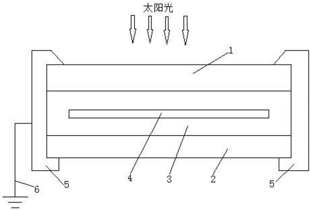
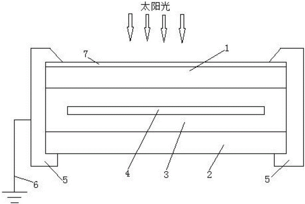
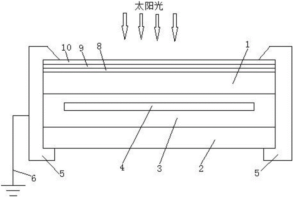
[0046] On the surface of a glass substrate with a thickness of 3mm, magnetron sputtering deposits a 20nm silicon oxide film layer as the first barrier layer 8; then, a 10nm Nb-doped titanium dioxide film is deposited on the silicon oxide film layer by magnetron sputtering layer as a conductive film layer 9; then on the Nb-doped titanium dioxide film layer, magnetron sputtering is used to deposit a 110nm silicon oxide film layer as a silicon-containing hydrophilic film layer 10; then the glass deposited with the above film layer is tempered and heat-treated , the tempered heat-treated glass is used as the cover glass 1 of the photovoltaic module, and the film layer on the surface of the tempered glass faces the light-receiving surface of the photovoltaic module, and at the same time, the metal frame 5 of the photovoltaic module is in contact with the Nb-doped titanium dioxide film layer 9 , thus forming the photovoltaic module of the present invention.
Embodiment 2
[0048] On the surface of a glass substrate with a thickness of 4mm, magnetron sputtering deposits a 25nm silicon oxynitride film layer as the first barrier layer 8; then adopts magnetron sputtering to deposit 15nm Ta-doped Titanium dioxide film layer is as conductive film layer 9; Then adopt magnetron sputtering to deposit 110nm silicon oxide film layer on Ta-doped titanium dioxide film layer as silicon-containing hydrophilic film layer 10; Then the glass that will be deposited with above-mentioned film layer is carried out Tempering heat treatment, the glass after tempering heat treatment is used as the cover glass 1 of the photovoltaic module, and the film layer on the surface of the tempered glass faces the light-receiving surface of the photovoltaic module, and at the same time, the metal frame 5 of the photovoltaic module and the Ta-doped titanium dioxide film layer 9 contact, thereby forming the photovoltaic module of the present invention.
Embodiment 3
[0050] On the surface of a glass substrate with a thickness of 4mm, magnetron sputtering deposits a 10nm zirconia film layer as the first barrier layer 8; then, a 5nm W-doped titanium dioxide film is deposited on the zirconia film layer by magnetron sputtering layer as a conductive film layer 9; then on the W-doped titanium dioxide film layer, a 105nm silicon oxide film layer is deposited by magnetron sputtering as a silicon-containing hydrophilic film layer 10; then the glass deposited with the above film layer is tempered and heat-treated , the tempered heat-treated glass is used as the cover glass 1 of the photovoltaic module, and the film layer on the surface of the tempered glass faces the light-receiving surface of the photovoltaic module, and at the same time, the metal frame 5 of the photovoltaic module is in contact with the W-doped titanium dioxide film layer 9 , thus forming the photovoltaic module of the present invention.
PUM
 Abstract
Description
Claims
Application Information
 - R&D
- Intellectual Property
- Life Sciences
- Materials
- Tech Scout
- Unparalleled Data Quality
- Higher Quality Content
- 60% Fewer Hallucinations
Browse by: Latest US Patents, China's latest patents, Technical Efficacy Thesaurus, Application Domain, Technology Topic, Popular Technical Reports.
© 2025 PatSnap. All rights reserved.Legal|Privacy policy|Modern Slavery Act Transparency Statement|Sitemap|About US| Contact US: help@patsnap.com


