InGaN/GaN multi-quantum well grown on glass substrate and preparation method therefor

A technology of glass substrate and multiple quantum wells, which is applied in the direction of electrical components, circuits, semiconductor devices, etc., can solve the problems of high price, high LED manufacturing cost, expensive sapphire and SiC substrates, etc., to achieve easy acquisition and reduce production cost, the effect of reducing the formation of dislocations

Active Publication Date: 2017-03-15
SOUTH CHINA UNIV OF TECH
View PDF3 Cites 3 Cited by
  • Summary
  • Abstract
  • Description
  • Claims
  • Application Information

AI Technical Summary

Problems solved by technology

Although the luminous efficiency of LED has surpassed that of fluorescent lamps and incandescent lamps, the luminous efficiency of commercial LEDs is still lower than that of sodium lamps (150lm / W), and the price per lumen / watt is relatively high.
At present, most GaN-based LEDs are based on epitaxial growth on sapphire and SiC substrates. Large-scale sapphire and SiC substrates are expensive, resulting in high LED manufacturing costs.

Method used


Image

  • InGaN/GaN multi-quantum well grown on glass substrate and preparation method therefor
  • InGaN/GaN multi-quantum well grown on glass substrate and preparation method therefor

Examples


Embodiment 1

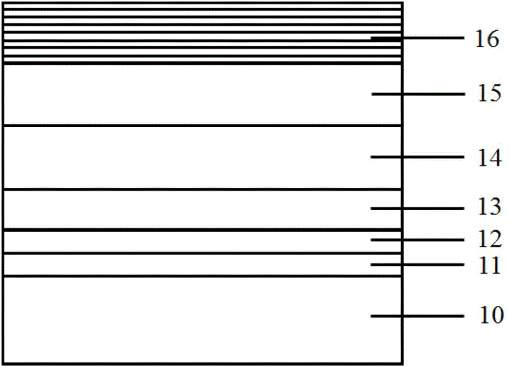
[0041] figure 1Shown is a schematic cross-sectional view of the InGaN / GaN multiple quantum well grown on a glass substrate prepared in this embodiment, as shown in the figure, including an aluminum metal layer 11 grown on a glass substrate 10, and grown on the aluminum metal layer 11 The silver metal layer 12, the AlN buffer layer 13 grown on the silver metal layer 12, the GaN buffer layer 14 grown on the AlN buffer layer 13, the non-doped GaN layer 15 grown on the GaN buffer layer 14, the non-doped GaN layer 15 grown on the non- Doping the InGaN / GaN multiple quantum wells 16 on the GaN layer 15 .

[0042] The preparation method of the InGaN / GaN multiple quantum well grown on the glass substrate of the present embodiment comprises the following steps:

[0043] (1) Selection of substrate: use ordinary glass substrate;

[0044] (2) Substrate surface polishing and cleaning treatment;

[0045] The surface polishing of the substrate is specifically:

[0046] First, the surface ...

Embodiment 2

[0057] The preparation method of the InGaN / GaN multiple quantum well grown on the glass substrate of the present embodiment comprises the following steps:

[0058] (1) Selection of substrate: use ordinary glass substrate;

[0059] (2) Substrate surface polishing and cleaning treatment;

[0060] The surface polishing of the substrate is specifically:

[0061] First, the surface of the glass substrate is polished with diamond slurry, and the surface of the substrate is observed with an optical microscope until there are no scratches, and then the chemical mechanical polishing method is used for polishing;

[0062] The cleaning is specifically:

[0063] Put the glass substrate into deionized water and ultrasonically clean it at room temperature for 5 minutes to remove the dirt particles on the surface of the glass substrate, then wash it with acetone and ethanol in sequence to remove the surface organic matter, and dry it with high-purity dry nitrogen;

[0064] (3) Growth of t...


PUM

PropertyMeasurementUnit
thicknessaaaaaaaaaa
thicknessaaaaaaaaaa
thicknessaaaaaaaaaa

Abstract

The invention discloses an InGaN/GaN multi-quantum well grown on a glass substrate. The InGaN/GaN multi-quantum well comprises an aluminum metal layer grown on the glass substrate, a silver metal layer grown on the aluminum metal layer, an AlN buffer layer grown on the silver metal layer, a GaN buffer layer grown on the AlN buffer layer, a non-doped GaN layer grown on the GaN buffer layer, and an InGaN/GaN quantum well grown on the non-doped GaN layer. The invention also discloses a preparation method for the InGaN/GaN multi-quantum well grown on the glass substrate. The multi-quantum well has the advantages of simple growth process and low preparation cost; and in addition, the prepared InGaN/GaN multi-quantum well is low in defect density, good in crystal quality, and good in electrical and optical performance.

Description

technical field [0001] The invention relates to an InGaN / GaN multi-quantum well and a preparation method, in particular to an InGaN / GaN multi-quantum well grown on a glass substrate and a preparation method. Background technique [0002] Light-emitting diode (LED), as a new type of solid-state lighting source and green light source, has outstanding features such as small size, low power consumption, environmental protection, long service life, high brightness, low heat and colorful, and is widely used in outdoor lighting, commercial lighting and decoration Engineering and other fields have a wide range of applications. At present, under the background of the increasingly serious problem of global warming, saving energy and reducing greenhouse gas emissions has become an important issue faced by the whole world. A low-carbon economy based on low energy consumption, low pollution, and low emissions will become an important direction of economic development. In the field of l...

Claims


Application Information

Patent Timeline
Patent Type & Authority Applications(China)
IPC IPC(8): H01L33/32H01L33/20H01L33/06H01L33/00H01L33/10
CPCH01L33/0093H01L33/06H01L33/10H01L33/20H01L33/32
Inventor 李国强高芳亮温雷
Owner SOUTH CHINA UNIV OF TECH
Why Eureka
Try Eureka