An ingot casting method for reducing the width of the red edge of a polycrystalline silicon ingot, a polycrystalline silicon ingot and a crucible for polycrystalline silicon ingot casting
A technology for polycrystalline silicon ingots and ingots, which is applied to the growth of polycrystalline materials, chemical instruments and methods, and crystal growth, can solve the problems of increasing the cost of casting ingots, increasing the cost of purchasing crucibles, and the high price of high-purity crucibles. The effects of lifespan, quality improvement, and reduction of red edge width
- Summary
- Abstract
- Description
- Claims
- Application Information
AI Technical Summary
Problems solved by technology
Method used
Image
Examples
Embodiment 1
[0109] An ingot casting method for reducing the width of the red edge of a polycrystalline silicon ingot, comprising the following steps:
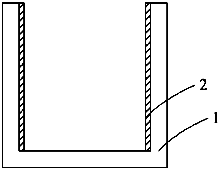
[0110] (1) Provide a crucible with an inner diameter of 840*840mm and a height of 480mm, spray a layer of silicon nitride coating on the side wall and base of the crucible, and let it dry naturally;
[0111] (2) Cut the high-purity graphite paper with a thickness of 200 μm into four rectangles whose specifications are respectively 780*300mm;
[0112] (3) Evenly smear one layer of high-purity silica sol on the high-purity graphite paper as a binding agent; four pieces of high-purity graphite paper coated with silica sol are attached to the four side walls of the crucible respectively to form a barrier layer;
[0113] (4) Install the seed crystal in the crucible, then fill the silicon material above the seed crystal, then control the temperature so that the silicon material melts from top to bottom, and after the silicon material melts to th...
Embodiment 2
[0118] An ingot casting method for reducing the width of the red edge of a polycrystalline silicon ingot, comprising the following steps:
[0119] (1) Provide a crucible with an inner diameter of 840*840mm and a height of 480mm, spray a layer of silicon nitride coating on the side wall and base of the crucible, and let it dry naturally;
[0120] (2) Provide nine*four rectangular high-purity graphite sheets with a thickness of 2mm and a length and width of 260*100mm;
[0121] (3) On nine pieces of high-purity graphite sheets, smear one layer of high-purity silica sol evenly as the binding agent respectively; High-purity graphite sheets coated with silica sol are also pasted on the other three side walls to form a barrier layer;
[0122] (4) Install the seed crystal in the crucible, then fill the silicon material above the seed crystal, then control the temperature so that the silicon material melts from top to bottom, and after the silicon material melts to the position of the...
Embodiment 3
[0127] An ingot casting method for reducing the width of the red edge of a polycrystalline silicon ingot, comprising the following steps:
[0128] (1) Provide a crucible with an inner diameter of 840*840mm and a height of 480mm, spray a layer of silicon nitride coating on the side wall and base of the crucible, and let it dry naturally;
[0129] (2) Provide two*four rectangular high-purity molybdenum sheets with a thickness of 50μm and a length and width of 390*300mm;
[0130] (3) On two high-purity molybdenum sheets, smear one layer of high-purity silica sol evenly as binding agent respectively; Two high-purity molybdenum sheets that are coated with silica sol are spliced and attached on one side wall of the crucible, similarly, High-purity molybdenum sheets coated with silica sol are also pasted on the other three side walls of the crucible to form a barrier layer;
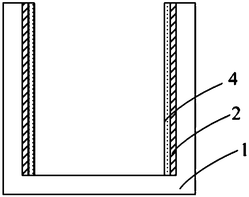
[0131] (4) setting a layer of silicon nitride layer on the barrier layer by spraying, the thickness of the...
PUM
| Property | Measurement | Unit |
|---|---|---|
| thickness | aaaaa | aaaaa |
| thickness | aaaaa | aaaaa |
| thickness | aaaaa | aaaaa |
Abstract
Description
Claims
Application Information


