Low on-resistance novel high-voltage SJ power device

A power device and a new type of technology, applied in the field of power semiconductor devices, can solve the problems of high specific on-resistance and low drift region, and achieve the effects of reducing specific on-resistance, increasing doping concentration, and uniform distribution of power lines

Inactive Publication Date: 2017-03-22
CHANGSHA UNIVERSITY OF SCIENCE AND TECHNOLOGY
View PDF4 Cites 9 Cited by
  • Summary
  • Abstract
  • Description
  • Claims
  • Application Information

AI Technical Summary

Problems solved by technology

But due to the low concentration in the drift region, the specific on-resistance is still high

Method used


Image

  • Low on-resistance novel high-voltage SJ power device
  • Low on-resistance novel high-voltage SJ power device
  • Low on-resistance novel high-voltage SJ power device

Examples


Embodiment 1

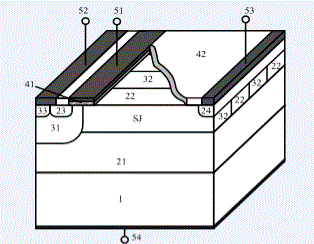
[0047] Embodiment 1: This embodiment provides a novel high-voltage SJ power device with low specific conductance, such as figure 2 As shown, its cellular structure includes a P-type substrate 1, an N-type drift region 21, a P-type buried layer 34, a P-type strip region 32, an N-type strip region 22, a P-type body region 31, and an N-type heavily doped region. 23. P-type heavily doped region 33, N-type heavily doped region 24, gate oxide layer 41, N-type buffer layer 25, polysilicon gate electrode 51, source terminal electrode 52, drain terminal electrode 53, substrate electrode 54, blunt The passivation layer 42, the source terminal field plate 55 and the drain terminal field plate 56. 42 is a passivation layer instead of a field oxide layer because the field oxide layer requires high temperature, which may cause the P / N strips to be dissipated, so the passivation layer is selected here 42. The N-type drift region 21 is provided with a P-type buried layer, and the drain end ...

Embodiment 2

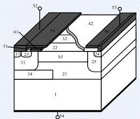
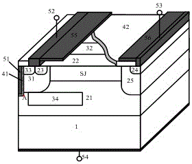
[0048] Embodiment 2: In order to solve the key technical problem of low specific conductance, this embodiment provides such as figure 2 In addition to the structures shown, three trench gate structures are also provided for comparison. Figure 7 It is an SJ device with a shallow trench gate structure. When the shallow trench gate device withstands voltage, the electric field in the drift region tends to be over-concentrated at the sharp corner of the trench oxide layer 41, as shown at point A in the figure, leading to premature breakdown of the device. Such as Figure 8 The medium groove gate structure extends a part of the polysilicon gate electrode into the N-type drift region 21 , and there is no other difference in structure between the medium groove gate device and the shallow groove gate device except for the depth of the groove gate. Compared with the shallow trench gate structure, the medium trench gate structure has two advantages: on the one hand, the trench gate a...

Embodiment 3

[0049] Embodiment 3: In order to thoroughly solve the problem of the substrate-assisted depletion effect, and at the same time improve the withstand voltage of the device. In addition to proposing figure 2 In addition to the structure shown, the N-type drift region 21 can also be in the form of linear variable doping, and the doping concentration increases sequentially from the source end to the drain end. The structure of a novel high-voltage SJ power device with low specific conductance provided by the present invention can be specifically applied to P-LDMOS, IGBT (Insulated Gate Bipolar Transistor, insulated gate bipolar transistor), SOI and PSOI (partial SOI) Lateral high-voltage devices with such structures. Such as Figure 12 As shown, a cross-sectional view of a lateral SJ LIGBT device structure provided by the present invention, wherein N-type heavily doped 24 at the drain end is replaced by P-type heavily doped 35; Figure 13 It is a structural diagram of a low on...


PUM


Abstract

The invention relates to a low on-resistance novel high-voltage SJ power device and belongs to the technical field of power semiconductor devices. In an N-type drift region of a transverse SJ power device, a P-type buried layer is introduced, a drain end is introduced into an N-type buffer layer, and a double field plate structure is introduced on the upper surface of the device. The P-type buried layer assists depletion of the N-type drift region, which increases the doping concentration of the drift region and reduces the on-resistance of the device. The N-type buffer layer of the drain end replaces an SJ structure under the drain end, which weakens the substrate-assisted depletion effect to some extent and can assist in depleting the P-type buried layer that is not completely depleted in the drift region, so that the super junction is enabled to never participate in vertical overvoltage resistance, thereby ensuring the charge balance of the super junction. The double field plate structure is a structure including double field plates which are a source end field plate and a drain end field plate. The field plates and device electrodes can be formed together without requiring other processing steps. The invention can improve the bulk electric field distribution and improve the overvoltage resistance of the device while reducing the on-resistance of the device. The invention can obtain various excellent transverse low on-resistance high-voltage SJ power devices with excellent performance.

Description

technical field [0001] The low specific conductance novel high-voltage SJ power device involved in the invention belongs to the technical field of power semiconductor devices. Background technique [0002] In the design of power MOSFET devices, the breakdown voltage BV and the specific on-resistance R on , sp The basic relationship is: R on , sp ∝BV 2.5 . The super-junction structure breaks the theoretical limit of conventional power MOSFET devices. While maintaining all the advantages of power MOSFETs, it significantly reduces its on-resistance, making R on , sp The relationship with BV has changed from 2.5 power to 1.32 power. The so-called super junction means that the drift region is changed from a single N or P to alternately composed of high-concentration N and P strips. When a reverse high voltage is applied, the N / P strips are mutually depleted to achieve a uniform distribution of equipotential lines in the drift region. . In the on-state of the n-type LD...

Claims


Application Information

Patent Timeline
Patent Type & Authority Applications(China)
IPC IPC(8): H01L29/78H01L29/06H01L29/40H01L29/739
CPCH01L29/0623H01L29/404H01L29/7393H01L29/7394H01L29/7816
Inventor 吴丽娟宋月章中杰杨航胡利民袁娜
Owner CHANGSHA UNIVERSITY OF SCIENCE AND TECHNOLOGY
Why Eureka
Try Eureka