Quantum dot luminescent layer and device, and preparation methods thereof, luminescence module and display device

A quantum dot luminescence and quantum dot technology, which is applied in semiconductor devices, electrical components, circuits, etc., can solve the problems of uneven luminescence, uneven thickness, and low performance of devices, and improve the uniformity and stability of luminescence. Effects of stabilization and improvement of luminous efficiency and luminous lifetime

Active Publication Date: 2017-03-22
TCL CORPORATION
View PDF3 Cites 22 Cited by
  • Summary
  • Abstract
  • Description
  • Claims
  • Application Information

AI Technical Summary

Problems solved by technology

[0006] In view of the above-mentioned deficiencies in the prior art, the object of the present invention is to provide a quantum dot cross-linked light-emitting layer and QLED device and its preparation method, a light-emitting module and a display device, aiming to solve the problems of uneven coverage and thickness of the existing quantum dot film layer. Inhomogeneity, and the problem of uneven light emission and lower performance of the device

Method used


Image

  • Quantum dot luminescent layer and device, and preparation methods thereof, luminescence module and display device
  • Quantum dot luminescent layer and device, and preparation methods thereof, luminescence module and display device
  • Quantum dot luminescent layer and device, and preparation methods thereof, luminescence module and display device

Examples


Embodiment 1

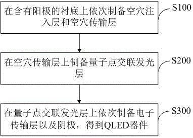
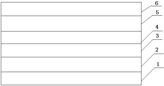
[0063] The preparation steps of the QLED device are as follows:

[0064] Spin-coat a layer of PEDOT:PSS thin film on the ITO substrate as the hole injection layer;

[0065] Spin-coat a layer of PVK on the PEDOT:PSS layer as a hole transport layer;

[0066] Spin-coat a layer of CdSe@ZnS coated with mercaptopropionic acid (MPA) ligands on the PVK layer as the quantum dot light-emitting layer;

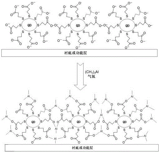
[0067] Next, the above-prepared CdSe@ZnS layer coated with mercaptopropionic acid (MPA) ligands was placed in a vacuum cavity, and trimethylaluminum ((CH 3 ) 3 Al) gas, where the internal pressure of the chamber is 0.05 mbar, the partial pressure of trimethylaluminum gas is 0.01 mbar, the internal temperature of the chamber is 16 °C, and the processing time is 5 min. Take it out after processing to obtain quantum dot crosslinking luminous layer;

[0068] Then, spin-coat one layer of ZnO on the quantum dot cross-linked luminescent layer prepared above as an electron transport layer;

...

Embodiment 2

[0071] The preparation steps of the QLED device are as follows:

[0072] Spin-coat a layer of PEDOT:PSS thin film on the ITO substrate as the hole injection layer;

[0073] Spin-coat a TFB layer on the PEDOT:PSS layer as a hole transport layer;

[0074] Spin-coat a layer of CdSe@ZnS coated with mercaptopropionic acid (MPA) ligands on the TFB layer as the quantum dot light-emitting layer;

[0075] Next, the above-prepared CdSe@ZnS layer coated with mercaptopropionic acid (MPA) ligands was placed in a vacuum cavity, and trimethylaluminum ((CH 3 ) 3 Al) gas, where the internal pressure of the cavity is 0.05 mbar, the partial pressure of trimethylaluminum gas is 0.02 mbar, the internal temperature of the cavity is 18 °C, and the processing time is 10 min. Take it out after processing to obtain quantum dot crosslinking luminous layer;

[0076] Then, spin-coat one layer of ZnO on the quantum dot cross-linked luminescent layer prepared above as an electron transport layer;

[00...

Embodiment 3

[0079] The preparation steps of the QLED device are as follows:

[0080] Spin-coat a layer of PEDOT:PSS thin film on the ITO substrate as the hole injection layer;

[0081] A layer of TFB was spin-coated on the PEDOT:PSS layer as a hole transport layer;

[0082] Spin-coat a layer of CdSe@ZnS coated with oleic acid (OA) ligand on the TFB layer as the quantum dot light-emitting layer;

[0083] Next, the above-prepared CdSe@ZnS layer coated with oleic acid (OA) ligands was placed in a vacuum chamber, and triethylaluminum ((CH 3 CH 2 ) 3 Al) gas, where the internal pressure of the cavity is 0.05 mbar, the partial pressure of triethylaluminum gas is 0.01 mbar, the internal temperature of the cavity is 18 °C, and the processing time is 20 min. Take it out after processing to obtain quantum dot crosslinking luminous layer;

[0084] Then, spin-coat one layer of ZnO on the quantum dot cross-linked luminescent layer prepared above as an electron transport layer;

[0085] Finally, ...


PUM

PropertyMeasurementUnit
concentrationaaaaaaaaaa

Abstract

The present invention discloses a quantum dot luminescent layer and device, and preparation methods thereof, a luminescence module and a display device. The preparation method of the quantum dot luminescent layer comprises the steps: the quantum dots having the surfaces coated with ligand are dissolved in solvent to obtain the quantum dot solution; the quantum dot solution is deposited on the substrate or a function layer by employing the solution method to obtain a quantum dot luminescent layer; the quantum dot luminescent layer is arranged in a vacuum cavity, and organic metal compounds are pumped in to process for 0.5-30 mins, wherein the pressure in the cavity is 0.01-1mbar, the partial pressure of the organic metal compounds after gasification is 0.001-0.1mbar, the temperature in the cavity is 10-25 DEG C; and the quantum dot luminescent layer is taken out to obtain the quantum dot crosslinking luminescent layer. The quantum dot film is not only uniform flat and has a stable film, so that the quantum dot film is difficult to be redissolved to take away or wash away by the solvent when the subsequent other function layers are deposited so as to effectively improve the luminescence uniformity and the stability of the QLED.

Description

technical field [0001] The invention relates to the technical field of light-emitting diodes, in particular to a quantum dot cross-linked light-emitting layer, a QLED device, a preparation method, a light-emitting module, and a display device. Background technique [0002] Quantum dots (Quantum dots, QDs), also known as semiconductor nanocrystals (Semiconductor nanocrystals), are semiconductor nanoparticles with a particle radius smaller than or close to the exciton Bohr radius, which have various unique optical properties, such as band gap The width is easy to tune, the absorption spectrum is wide, the spectral purity is high, and the optical / chemical performance is stable. Quantum dot light-emitting diodes (QLEDs) based on quantum dots are called quantum dot light-emitting diodes (Quantum dot light-emitting diodes, QLEDs). Compared with traditional light-emitting diodes and OLEDs, QLED has outstanding advantages such as high color purity, good stability, long life, good c...

Claims


Application Information

Patent Timeline
Patent Type & Authority Applications(China)
IPC IPC(8): H01L33/04H01L33/26H01L33/00
Inventor 梁柱荣曹蔚然
Owner TCL CORPORATION
Why Eureka
Try Eureka