

High strength photonic crystal membrane and manufacture method therefor
A photonic crystal, high-strength technology, applied in optics, optical components, instruments, etc., can solve the problems of photonic crystal structure damage, limited monomers that can be photo-initiated polymerization, etc., and achieve a strong practical effect
- Summary
- Abstract
- Description
- Claims
- Application Information
AI Technical Summary
Problems solved by technology
Method used
Image

Examples
Embodiment 1
[0030] Preparation of CdS / nitrovarnish high-intensity photonic crystal films.
[0031] Firstly, monodisperse CdS colloidal microspheres are prepared, and the specific preparation method is as follows:
[0032] Weigh 0.6 g of polyvinylpyrrolidone powder (PVP), add 30 mL of diethylene glycol, and then add a certain amount of cadmium nitrate and thiourea powder to make the concentration of cadmium nitrate and thiourea 0.1 M, and stir until all the powders are completely dissolved. The solution was heated to 150° C., incubated for 1 h, and then cooled to room temperature naturally. The product was centrifuged, washed with water three times, and dried.
[0033] A certain amount of monodispersed CdS microsphere powder was weighed, and absolute ethanol was added to prepare a dispersion liquid with a concentration of 10 wt%.
[0034] A certain amount of nitro varnish was dropped on the cleaned glass sheet, and it was used as an assembly substrate after natural drying at room temperat...
Embodiment 2
[0038] Preparation of CdS / PMMA high-strength photonic crystal films.
[0039] The CdS dispersion in Comparative Example 1 was used for the preparation of photonic crystal films. PMMA was used as the polymer component, and the solution was dissolved in THF to prepare a solution with a mass fraction of 20%, which was added dropwise to a glass plate after natural drying at room temperature for 0.5h as an assembly. base use. The ethanol dispersion of CdS microspheres was dropped on the partially dried PMMA film to completely cover the surface of the polymer film, and the whole was placed on a heating plate with a temperature of 80 °C. After the solvent was completely evaporated, high strength was obtained. Photonic crystal film.
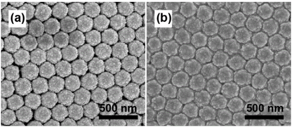
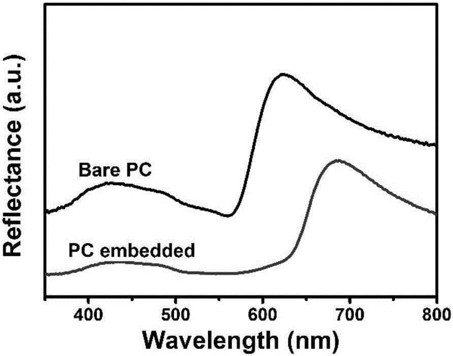
[0040] figure 1 The scanning electron microscope images of the photonic crystal film obtained by the direct assembly of CdS microspheres in Example 1 and the photonic crystal film wrapped in the nitro varnish film, as shown in the figure, when there is...
PUM
| Property | Measurement | Unit |
|---|---|---|
| particle diameter | aaaaa | aaaaa |
Abstract
Description
Claims
Application Information