
Transparent conductive film and manufacturing method therefor, and touch screen

A technology of transparent conductive film and production method, which is applied in the direction of transparent dielectric, printed circuit manufacturing, conductive pattern formation, etc., can solve the problem of non-bending, inability to meet small quantity, variety, low-cost and rapid manufacturing, unfavorable industrial production and sales, etc. question

Active Publication Date: 2017-03-29
SUZHOU WEIYEDA TOUCH TECH +1
View PDF2 Cites 22 Cited by
  • Summary
  • Abstract
  • Description
  • Claims
  • Application Information

AI Technical Summary

Problems solved by technology

The current mainstream capacitive touch panel mainly has a layer of indium tin oxide (ITO) conductive film on the inner surface of the glass screen and the interlayer. Since indium is a rare element, it is expensive and has a high resistance value, so it cannot be bent. It is not conducive to industrial production and sales, and another capacitive touch panel uses nano-silver metal grids to make conductive films, which emboss the required metal grid grooves on the polymer surface by means of mold embossing , and then filled with nano-silver material to form a conductive film, however
Different models and different manufacturers of conductive films have different circuit designs, and molds with different graphics need to be made according to their requirements. However, the cost of molds is high, and the development cycle is relatively long, which cannot meet the needs of small and diverse product production. , low cost, rapid manufacturing and other requirements

Method used


Image

  • Transparent conductive film and manufacturing method therefor, and touch screen
  • Transparent conductive film and manufacturing method therefor, and touch screen
  • Transparent conductive film and manufacturing method therefor, and touch screen

Examples


Embodiment Construction

[0040] Preferred embodiments of the present invention will be described in detail below in conjunction with the accompanying drawings.

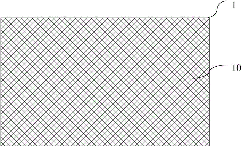
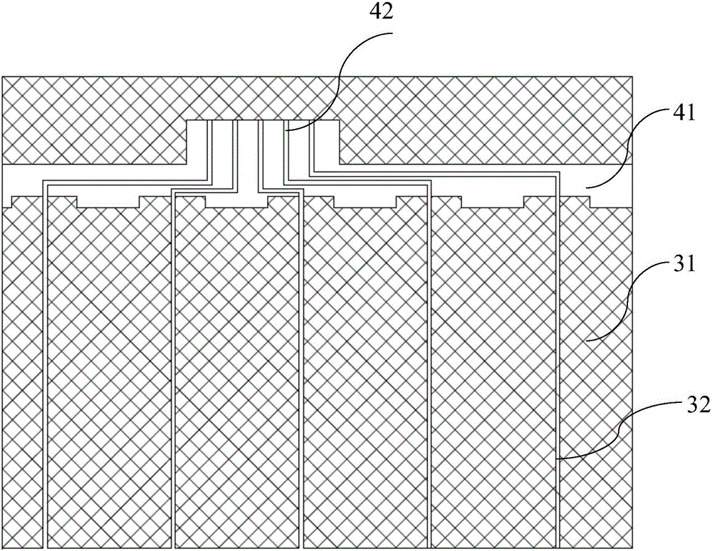
[0041] A transparent conductive film. The transparent conductive film is divided into a conductive area and a non-conductive area. The conductive area is composed of an inner line and an outer line. There are grid lines in the non-conductive area, and there is no conductive material in the groove of the grid line. In a preferred embodiment, the circuit channels in the conductive region are divided by laser or etching, and the division interval is preferably 20 microns. The grid of the conductive area can be in any shape, such as: square, rectangle, rhombus, diamond, pentagon, hexagon, random grid, etc. The routing method of the dividing line can be single or multiple straight lines, oblique lines, and is not limited by the shape of the channel. The grid line is a buried groove structure, which belongs to the metal grid structure.

[0042] r...


PUM

PropertyMeasurementUnit
depthaaaaaaaaaa
widthaaaaaaaaaa
thicknessaaaaaaaaaa

Abstract

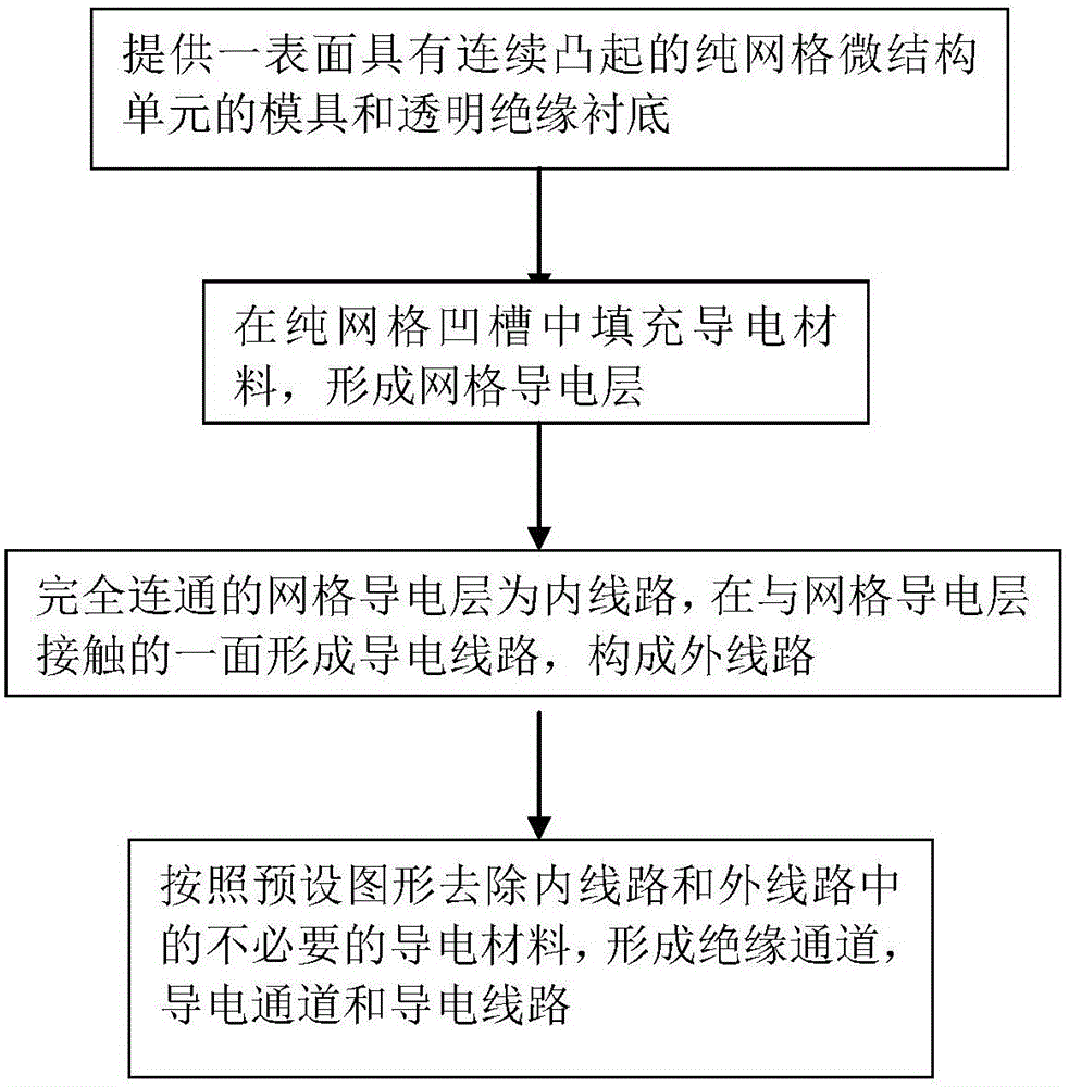
The invention discloses a transparent conductive film and a manufacturing method therefor, and a touch screen. The manufacturing method comprises the steps of performing imprinting on one surface of a transparent insulating substrate by a die to form continuous grooves; coating one surface of the transparent insulating substrate with jelly, and performing imprinting on one surface far from the transparent insulating substrate by a die, and curing to form grooves; filling the grooves with a conductive material to form a conductive layer, namely an internal circuit; forming an external circuit on one surface in contact with the conductive layer; and removing unnecessary conductive materials from the internal circuit and the external circuit according to a preset pattern to form insulating channels and insulating circuits so as to complete the manufacturing of the transparent conductive film. According to the manufacturing method, silk-screen printing and embedded type nanometer imprint are combined, and unified grid filling is used as the universal die; and the die is applicable to multiple types of machines, and only silk-screen printing and laser are needed according to different specifications, so that cost can be effectively lowered and the development period can be effectively shortened.

Description

technical field [0001] The invention relates to the field of touch screens, in particular to a method for manufacturing a transparent conductive film with a touch function, and a transparent conductive film and a touch screen prepared by the method. Background technique [0002] With the development of science and technology, more and more consumer electronic products, such as mobile phones, tablet computers, home appliances and other products, are operated with touch screens on the surface. As a new computer input device, the touch panel is currently the simplest, A convenient and natural way of human-computer interaction. Existing touch panels are distinguished according to their principles, including resistive technology, capacitive technology, infrared technology, and surface acoustic wave technology. The current mainstream capacitive touch panel mainly has a layer of indium tin oxide (ITO) conductive film on the inner surface and interlayer of the glass screen. Since i...

Claims


Application Information

Patent Timeline
Patent Type & Authority Applications(China)
IPC IPC(8): G06F3/041
CPCG06F3/041G06F2203/04103G06F2203/04112H05K3/107H05K3/12H05K2201/0391H05K2201/0108G06F3/044H05K3/0014H05K3/02Y10T29/49155
Inventor 周小红王涛吴革明谢文肖江梅陈林森
Owner SUZHOU WEIYEDA TOUCH TECH
Learn More