

Full-back-contact high-efficiency crystalline silicon cell metal graphical making method
A technology of full back contact and crystalline silicon cells, applied in the field of solar cells, can solve the problems of unsuitability for mass production, self-alignment compensation doping, high precision requirements, etc., achieve FF and Voc improvement, reduce preparation costs, align Effects with low precision requirements
- Summary
- Abstract
- Description
- Claims
- Application Information
AI Technical Summary
Problems solved by technology
Method used
Image

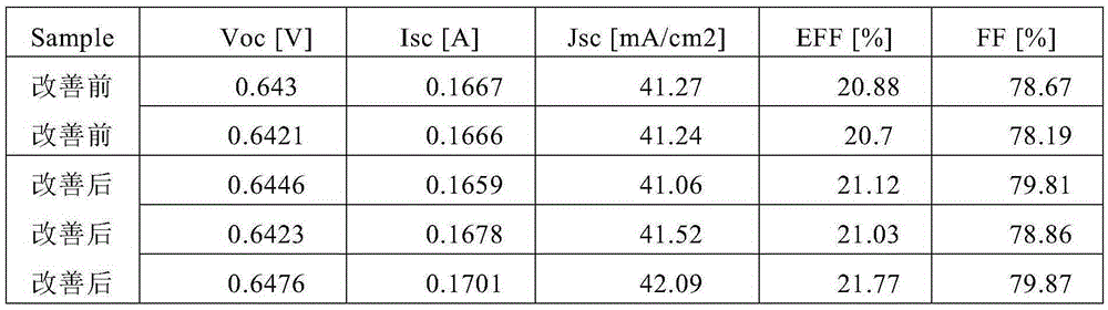
Examples
Embodiment 1
[0021] A full-back contact high-efficiency crystalline silicon battery metal patterning method, for full-back contact crystalline silicon batteries, perform high-temperature boron diffusion on the back to form an emitter junction, back phosphorus diffusion to form a back surface field, front surface phosphorus diffusion front surface field, and front / back passivation The anti-reflection layer deposition process also includes the electrode pattern and metallization process, and the following steps are adopted:
[0022] (1) The surface passivation layer is patterned and opened in the emitter junction area and the back surface field area of the full back contact cell, and the dry method is used to peel off the openings of the passivation layer to uniformly or unevenly distribute round holes, continuous or irregular Continuous rectangle, square or irregular pattern, but the first prerequisite is to meet the subsequent metallization requirements, and the peeling size of the passiv...
Embodiment 2
[0027] A full-back contact high-efficiency crystalline silicon battery metal patterning method, for full-back contact crystalline silicon batteries, perform high-temperature boron diffusion on the back to form an emitter junction, back phosphorus diffusion to form a back surface field, front surface phosphorus diffusion front surface field, and front / back passivation The anti-reflection layer deposition process also includes the electrode pattern and metallization process, and the following steps are adopted:
[0028] (1) In the emitter junction area and the back surface field area of the full back contact battery, the surface passivation layer is patterned and opened, and the passivation layer is peeled off with uniform or uneven distribution of round holes, continuous or uneven Continuous rectangle, square or irregular pattern, but the first premise is to meet the subsequent metallization requirements, the peeling size of the passivation layer is 100μm,
[0029] (2) Use a ...
Embodiment 3
[0034] A full-back contact high-efficiency crystalline silicon battery metal patterning method, for full-back contact crystalline silicon batteries, perform high-temperature boron diffusion on the back to form an emitter junction, back phosphorus diffusion to form a back surface field, front surface phosphorus diffusion front surface field, and front / back passivation The anti-reflection layer deposition process also includes the electrode pattern and metallization process, and the following steps are adopted:
[0035] (1) In the emitter junction area and the back surface field area of the full back contact cell, the surface passivation layer is patterned and opened, and laser treatment is used, and the openings of the passivation layer are peeled off uniformly or unevenly distributed circular holes, continuous or discontinuous Rectangular, square or irregular patterns, but the first premise is to meet the subsequent metallization requirements, the peeling size of the passivat...
PUM
 Abstract
Description
Claims
Application Information