Quantum-dot Light-Emitting Diode (QLED) device based on p-i-n structure and fabrication method of QLED device

A p-i-n device technology, applied in the field of quantum dots, can solve the problems of poor stability, low luminous efficiency and short service life of quantum dot devices, and achieve the effects of reducing quenching, reducing cross-relaxation and improving current efficiency

Inactive Publication Date: 2017-03-29
TCL CORPORATION
View PDF9 Cites 23 Cited by
  • Summary
  • Abstract
  • Description
  • Claims
  • Application Information

AI Technical Summary

Problems solved by technology

[0006] In view of the above-mentioned deficiencies in the prior art, the purpose of the present invention is to provide a QLED device based on p-i-n structure and its preparation method, aiming at solving the problem that existing qu

Method used


Image

  • Quantum-dot Light-Emitting Diode (QLED) device based on p-i-n structure and fabrication method of QLED device
  • Quantum-dot Light-Emitting Diode (QLED) device based on p-i-n structure and fabrication method of QLED device

Examples


Embodiment 1

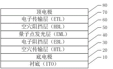
[0041] In a QLED, glass substrate, 120nm ITO; HTL is F4-TCNQ:TFB=1:10, thickness is 25nm; EBL is TFB, EBL thickness is 15nm; i-EML is a quantum dot layer ( CdSe / ZnS) QDs / PMMA, the weight percentage of quantum dot material CdSe / ZnS and host material PMMA is 10:1, and the thickness is 40 nanometers; HBL is nano-zinc oxide, and the thickness is 10 nanometers; ETL is aluminum-doped zinc oxide, The doping concentration is 5wt%, the thickness is 20nm; the electrode is Al.

Embodiment 2

[0043] In a QLED, glass substrate, 120nm ITO; HTL is Cu:MoO 3 =10wt%, thickness is 25nm; EBL is MoO 3 , EBL thickness is 10nm; i-EML is the quantum dot layer (CdSe / ZnS) QDs / PMMA introduced into the intrinsic host material PMMA, the weight percentage of quantum dot material CdSe / ZnS and host material PMMA is 10:1, and the thickness is 40 nanometer; HBL is nano-zinc oxide with a thickness of 10 nanometers; ETL is lithium-doped zinc oxide with a doping concentration of 5% and a thickness of 20 nm; the electrode is Al.

Embodiment 3

[0045] In a QLED, glass substrate, 120nm ITO; HTL is F4-TCNQ:TFB = 1:10, thickness is 25nm; EBL is TFB, EBL thickness is 15nm; i-EML is the introduction of intrinsic matrix material SiO 2 Quantum dot layer of sol (CdSe / ZnS) QDs / SiO 2 , quantum dot material CdSe / ZnS and host material SiO 2 The weight percentage is 10:1, and the thickness is 40 nm; HBL is nano-zinc oxide, with a thickness of 10 nm; ETL is aluminum-doped zinc oxide, with a doping concentration of 5wt% and a thickness of 20 nm; the electrode is Al.

[0046] To sum up, the present invention provides a QLED device based on a p-i-n structure. On the one hand, the driving voltage of the QLED device is reduced by using a p-type material as a hole transport layer and an n-type material as an electron transport layer, thereby effectively reducing the Quenching of the luminescence of quantum dots by the Stark effect; on the other hand, the cross-relaxation between quantum dots can be reduced by introducing intrinsic hos...


PUM

PropertyMeasurementUnit
Thicknessaaaaaaaaaa

Abstract

The invention discloses a quantum-dot light-emitting diode (QLED) device based on a p-i-n structure and a fabrication method of the QLED device. The QLED device comprises a substrate, a bottom electrode, a hole transmission layer, an electron blocking layer, a quantum-dot light-emitting layer, a hole blocking layer, an electron transmission layer and a top electrode. On one hand, the driving voltage of the QLED device is reduced by taking p-type material as the hole transmission layer and an n-type material as the electron transmission layer, so that the quenching of a Stark effect on quantum-dot light emitting is effectively reduced; on the other hand, cross relaxation among quantum dots is reduced by introducing an intrinsic matrix material into the quantum-dot light-emitting layer, and the radiation combination probability is improved; and meanwhile, injected electrons and holes can also be effectively captured to improve current efficiency, so that the light-emitting efficiency of the device and the stability of the device are improved, and the service lifetime of the device is prolonged.

Description

technical field [0001] The invention relates to the technical field of quantum dots, in particular to a QLED device based on a p-i-n structure and a preparation method thereof. Background technique [0002] For solid-state lighting and display technology, how to reduce the driving voltage to obtain devices with low power consumption has always been a difficult problem for researchers to solve. In the prior art, the electrical conductivity is usually improved by heavily doped transport materials, thereby effectively reducing the driving voltage of the device; devices with low driving voltage and low energy consumption have been obtained by using p-i-n technology in OLEDs. The highly conductive p-type heavily doped and n-type heavily doped transport layers can effectively enhance electrical injection and reduce the ohmic loss of the transport layer during device driving. [0003] For group II and group VI luminescent quantum dots, the luminous efficiency is high, the color pu...

Claims


Application Information

Patent Timeline
IPC IPC(8): H01L51/50H01L33/06
CPCH01L33/06H10K50/115H10K50/155H10K50/165
Inventor 钱磊杨一行曹蔚然向超宇陈崧
Owner TCL CORPORATION
Why Eureka
Try Eureka