An integral silicon carbide Darlington tube and its manufacturing method

A Darlington tube, integrated technology, applied in the field of microelectronics, can solve the problems of complex manufacturing process, small current handling capacity of the drive tube, and high cost

Active Publication Date: 2019-10-01
XIDIAN UNIV
View PDF2 Cites 0 Cited by
  • Summary
  • Abstract
  • Description
  • Claims
  • Application Information

AI Technical Summary

Problems solved by technology

[0005] To sum up, the existing silicon carbide Darlington tube has the problem of relatively small current handling capacity of the drive tube and complicated manufacturing process, resulting in relatively high cost.

Method used


Image

  • An integral silicon carbide Darlington tube and its manufacturing method
  • An integral silicon carbide Darlington tube and its manufacturing method
  • An integral silicon carbide Darlington tube and its manufacturing method

Examples


Embodiment 1

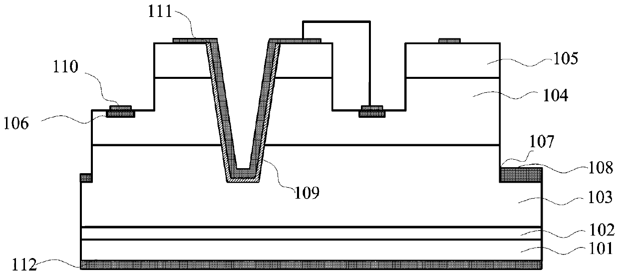
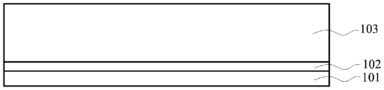
[0050] In the first step, an N+ buffer layer 102 is epitaxially grown on the N+ substrate 101 . Specifically, as Figure 2A As shown in the figure, the N+ substrate 101 was first cleaned by RCA standard; then, the front surface of the N+ substrate 101 was epitaxially grown by a low-pressure hot-wall chemical vapor deposition method with a thickness of 3.5 μm and a nitrogen ion doping concentration of 8×10 17 cm -3 The N+ buffer layer 102.

[0051] It should be noted that the growth conditions of the N+ buffer layer 102 are as follows: the temperature is 1600° C., the pressure is 100 mbar, the reaction gas includes silane and propane, the carrier gas is pure hydrogen, and the impurity source is liquid nitrogen.

[0052] It should be noted that the RCA standard cleaning method was pioneered in 1965 by Kern and Puotinen et al. in the RCA laboratory in N.J.Princeton, from which it was named. RCA is a typical and still the most commonly used wet chemical cleaning method. The cle...

Embodiment 2

[0087] In step 1, an N+ buffer layer 102 is epitaxially grown on the N+ substrate 101 . Specifically, as Figure 2A As shown in the figure, the N+-type silicon carbide substrate 10 is firstly cleaned by RCA standard; 18 cm -3 the buffer layer 102 .

[0088] It should be noted that the growth conditions of the N+ buffer layer 102 are as follows: the temperature is 1600° C., the pressure is 100 mbar, the reaction gas includes silane and propane, the carrier gas is pure hydrogen, and the impurity source is liquid nitrogen.

[0089] Step 2, epitaxially growing the N- collector region 103 on the N+ buffer layer 102, specifically, as Figure 2B As shown, on the buffer layer 102, the epitaxial growth thickness is 100 μm by the low pressure hot-wall chemical vapor deposition method, and the nitrogen ion doping concentration is 2×10 14 cm -3 The N-collector region 103.

[0090] It should be noted that the growth process conditions of the N-collector region 103 are as follows: the...

Embodiment 3

[0116] In step A, the N+ buffer layer 102 is epitaxially grown on the N+ substrate 101 . Specifically, as Figure 2AAs shown in the figure, the N+-type silicon carbide substrate 10 is first cleaned by RCA standard; 18 cm -3 the buffer layer 102 .

[0117] It should be noted that the growth conditions of the N+ buffer layer 102 are as follows: the temperature is 1600° C., the pressure is 100 mbar, the reaction gas includes silane and propane, the carrier gas is pure hydrogen, and the impurity source is liquid nitrogen.

[0118] Step B, epitaxially growing the N- collector region 103 on the N+ buffer layer 102, specifically, as Figure 2B As shown, on the buffer layer 102, the epitaxial growth thickness is 105 μm by the low pressure hot-wall chemical vapor deposition method, and the nitrogen ion doping concentration is 6×10 14 cm -3 The N-collector region 103.

[0119] It should be noted that the growth process conditions of the N-collector region 103 are as follows: the t...


PUM

PropertyMeasurementUnit
widthaaaaaaaaaa
thicknessaaaaaaaaaa
thicknessaaaaaaaaaa

Abstract

The invention discloses an integrated silicon carbide Darlington transistor and a manufacturing method thereof, and belongs to the technical field of micro-electronics, aiming at addressing the problems of small capability of driving tube current handling, complex manufacturing technologies, and high cost of current silicon carbide Darlington transistors. The integrated silicon carbide Darlington transistor includes: a N+emitting region which is arranged on the upper surface of a base region and includes a device slot which assumes the shape of a tilted slot, a device isolation region which assumes the shape of a vertical slot and an emitting region table which assumes the shape of a vertical slot; a base region P+ injection region which is arranged on a lower surface of the emitting region table and is disposed within the base region, wherein the device slot is arranged in the N+emitting region and extends to the upper portion of a N-collector region, the device isolation region is arranged in the N+emitting region and extends to the upper portion of the N-collector region; and an isolation injection layer which is arranged on the upper surface of the bottom portion of the device isolation region.

Description

technical field [0001] The invention belongs to the technical field of microelectronics, and relates to a semiconductor device, in particular to an integral silicon carbide Darlington tube and a manufacturing method thereof. Background technique [0002] With the rapid development of power electronics technology, the demand for high-power semiconductor devices is becoming more and more significant. Due to the limitation of materials, the characteristics of traditional silicon devices have reached their theoretical limits. Silicon carbide is a wide-bandgap semiconductor material developed rapidly in the past decade. It has wide-bandgap, high thermal conductivity, and high carrier saturation migration. It has the advantages of high power efficiency, high power density, etc., and can be suitable for applications such as high power, high temperature and radiation resistance. Among them, the switching device based on oxide layer MOSFET (English: Metal-Oxide-Semiconductor Field-E...

Claims


Application Information

Patent Timeline
Patent Type & Authority Patents(China)
IPC IPC(8): H01L27/082H01L29/08H01L21/8222
Inventor 元磊李钊君宋庆文汤晓燕张艺蒙张玉明
Owner XIDIAN UNIV
Why Eureka
Try Eureka