A Tunneling Field Effect Transistor Effectively Increases On-state Current

A technology of tunneling field effect and on-state current, which is applied in the direction of circuits, electrical components, semiconductor devices, etc., can solve the problems of limiting tunneling current, electric field limitation, and line tunneling cannot occur, so as to increase the on-state current, The effect of increasing the electric field and increasing the intensity

Active Publication Date: 2021-03-30
UNIV OF ELECTRONICS SCI & TECH OF CHINA
View PDF10 Cites 0 Cited by
  • Summary
  • Abstract
  • Description
  • Claims
  • Application Information

AI Technical Summary

Problems solved by technology

Due to the symmetrical distribution of the upper and lower gate electrodes, the electric field in the vertical direction is limited. When the channel thickness is small, line tunneling cannot occur, thus limiting the tunneling current.

Method used


Image

  • A Tunneling Field Effect Transistor Effectively Increases On-state Current
  • A Tunneling Field Effect Transistor Effectively Increases On-state Current
  • A Tunneling Field Effect Transistor Effectively Increases On-state Current

Examples


Embodiment 1

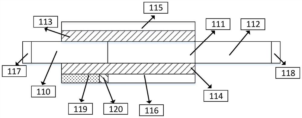
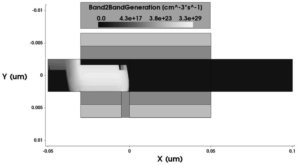
[0020] In Example 1, the thickness of the source region, the channel region and the drain region are all 5nm, and the doping concentration is 1E20cm -3 P-type doping, 1E15cm -3 N-type doping and 5E18cm -3 N-type doping. The metal gate and the bias electrode partially covered by the source region enhance the electric field in the vertical direction of the source region, so that the carriers in the source region can undergo line tunneling, thereby effectively increasing the on-state current.

Embodiment 2

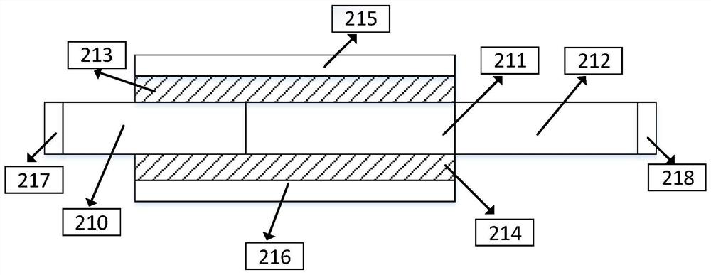
[0021] In Example 2, the thickness of the source region, the channel region and the drain region are all 7nm, and the doping concentration is 1E20cm -3 P-type doping, 1E15cm -3 N-type doping and 5E18cm -3 N-type doping. It is used to illustrate the ability of the present invention to increase the on-state current under different channel thicknesses.

Embodiment 3

[0022] In Example 3, the thickness of the source region, the channel region and the drain region are all 5nm, and the doping concentration is 1E20cm -3 P-type doping, 1E15cm -3 N-type doping and 5E18cm -3 N-type doping. The material of the bias electrode in Example 3 is gold, and its work function difference is larger than that of the gate electrode, which is used to illustrate that the difference in metal work function between electrode materials can be used to achieve the same effect as an external bias voltage.

[0023] figure 1 It is a structural schematic diagram of a tunneling field effect transistor that effectively increases the on-state current provided in the first embodiment. The transistor comprises a source region (110), a channel region (111), a drain region (112), a top gate dielectric layer (113) and a bottom gate dielectric layer (114), a top metal gate (115) and a bottom metal gate (116 ), a bias electrode (119), a source electrode (117), a drain electrod...


PUM

PropertyMeasurementUnit
thicknessaaaaaaaaaa
lengthaaaaaaaaaa
lengthaaaaaaaaaa

Abstract

The invention discloses a tunneling field effect transistor for effectively increasing the on-state current, which belongs to the field of semiconductor devices and is used for increasing the on-state current of the tunneling field effect transistor. In the present invention, the upper and lower gate dielectric layers of the tunneling field effect transistor are extended to the source region and partly covered to the source region, the surface of the gate dielectric layer on one side of the source region is covered with a metal gate, and the surface of the gate dielectric layer on the other side of the source region is covered with a bias electrode , the bias electrode and the metal grid on this side are separated by a partition wall to form an up-and-down asymmetric structure. By applying a bias voltage to the bias electrode, or using the metal work function difference between the bias electrode and the metal grid, the gate electrode is enhanced. The electric field perpendicular to the channel direction on the upper and lower sides of the covered part of the source region increases the strength of the carrier line tunneling, and the total carrier tunneling area and tunneling probability increase, thereby effectively increasing the device's on-state current.

Description

technical field [0001] The invention belongs to the field of semiconductor devices and relates to a tunneling field effect transistor, in particular to a tunneling field effect transistor capable of effectively increasing the on-state current. Background technique [0002] Tunneling Field Effect Transistor (TFET) is based on the working principle of band-band tunneling, and its subthreshold swing can break through the theoretical limit of 2.3kT / q of MOSFET subthreshold swing, which is 60mV / dec at room temperature. Taking N-type TFET as an example, the source region is heavily doped with P type, the channel region is lightly doped with N type, and the drain region is heavily doped with N type, the source is connected to low potential, and the drain is connected to high potential. When a positive voltage is applied to the gate electrode, the energy band of the channel region drops, and when the conduction band of the channel region drops below the valence band of the source re...

Claims


Application Information

Patent Timeline
Patent Type & Authority Patents(China)
IPC IPC(8): H01L29/78H01L29/423
CPCH01L29/42356H01L29/7831
Inventor 谢倩夏霜李杰王政
Owner UNIV OF ELECTRONICS SCI & TECH OF CHINA
Why Eureka
Try Eureka