MEMS (Micro-Electro-Mechanical System) cutting and cleaning as well as releasing method of wafer

A wafer and cutting blade technology, applied in the field of MEMS wafer cutting, cleaning and releasing, can solve the problems of easy touch of chips, low production efficiency, expensive thinning equipment and plasma cutting equipment, etc., and achieve the effect of good uniformity

Inactive Publication Date: 2017-05-10
YANTAI RAYTRON TECH
View PDF12 Cites 4 Cited by
  • Summary
  • Abstract
  • Description
  • Claims
  • Application Information

AI Technical Summary

Problems solved by technology

[0007] 2) Release the structure of the wafer first, punch holes and stick film to protect the MEMS structure of the wafer, and then perform back cutting; due to the film protection of the MEMS structure of the wafer, additional processes are required and the process is complicated, and the problem of back cutting is cost High, low operating efficiency, unstable yield rate, not suitable for chips with high proportion of MEMS
[0008] 3) Protect the front of the wafer with glue first, then perform photolithography, use plasma cutting to cut, and then release; photolithography is required, and thinning is required before release, photolithography equipment, thinning equipment and Plasma cutting equipment is very expensive
[0009] Comparative document Chinese patent CN 103068318 A discloses a MEMS silicon wafer wafer cutting and structure release method. The obvious problem is that wafer-level operations have not been realized. Silicon wafers need to be filmed twice and manually split, using a vacuum suction pen Pick up a single chip, and then put it on the tray to remove the glue, and a silicon wafer contains thousands of chips, and the single pick-up efficiency is low; and this reference document does not disclose the cleaning method of the wafer. For round cleaning, the chip is removed, placed in a tray and placed in a solution for cleaning. The chips are easy to touch and damage the chip. In addition, the two cuts in the comparison file are at the same position, and the cutting positions are strictly aligned. , but after cutting once, cutting again from the beginning requires two alignments, and the two alignment cutting positions cannot be completely overlapped, and the production efficiency is low

Method used


Image

  • MEMS (Micro-Electro-Mechanical System) cutting and cleaning as well as releasing method of wafer
  • MEMS (Micro-Electro-Mechanical System) cutting and cleaning as well as releasing method of wafer
  • MEMS (Micro-Electro-Mechanical System) cutting and cleaning as well as releasing method of wafer

Examples


Embodiment Construction

[0044] The principles and features of the present invention are described below in conjunction with the accompanying drawings, and the examples given are only used to explain the present invention, and are not intended to limit the scope of the present invention.

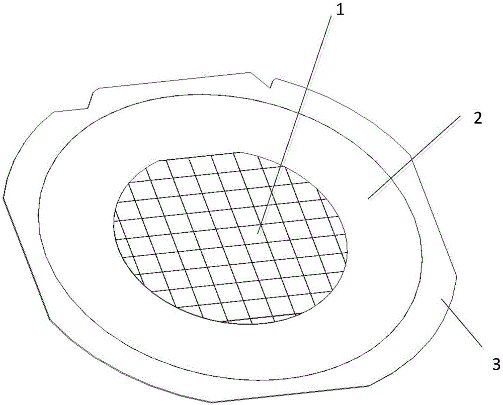
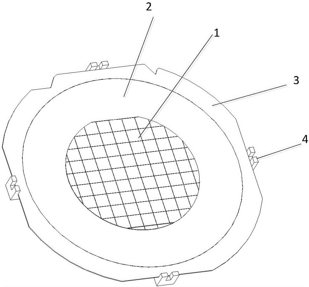
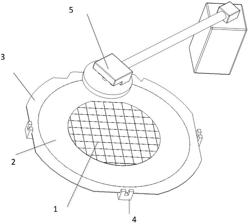
[0045] Such as Figure 1-Figure 4 Shown, a kind of MEMS wafer cutting cleaning and release method, comprises the following steps:

[0046] Step 1: Paste the UV film 2, place the wafer 1 face down on the center of the suction cup of the film mounter, the suction cup is a vacuum suction cup suspended in the middle; pull out the UV film from the rear drum of the film mounter, the length exceeds the stainless steel frame The outer circumference of 3 is 2 to 10 cm. If there are wrinkles locally, it needs to be further tightened until the surrounding area is even and flat, and then gently push the film with a roller to make the film flat and close to the back of wafer 1 and stainless steel frame 3; UV film 2 is cut off, ...


PUM

PropertyMeasurementUnit
thicknessaaaaaaaaaa
thicknessaaaaaaaaaa
depthaaaaaaaaaa

Abstract

The invention relates to an MEMS (Micro-Electro-Mechanical System) cutting and cleaning as well as releasing method of a wafer. The method comprises the following steps of pasting a UV (Ultraviolet) film, wherein the frontal surface of the wafer is put at the midpoint of a vacuum suction cup, of which the middle is suspended, of a film pasting machine; cutting, wherein a step cutting is adopted, the two-step cutting is continuously completed, the cutting thickness of a front cutting blade is 20 to 60 percent of the total thickness of the wafer, and a back cutting blade is used for thoroughly scratching the wafer; cleaning and spin-drying, wherein the wafer which is fixedly arranged on a stainless steel frame is integrally placed on a rotatable ceramic dense-hole suction cup, the ceramic dense-hole suction cup is used for fixing the periphery of the stainless steel frame, a liquid spraying system is arranged above the ceramic dense-hole suction cup, the liquid spraying system comprises a plurality of spray heads capable of leftwards and rightwards swinging to spray a solution, the spray heads spray liquid to clean the wafer, and the ceramic dense-hole suction cup is rotated at a high speed, so as to throw out waste liquid; irradiating; carrying out film expansion on the wafer; taking down a chip from the UV film by utilizing a chip pick-up device, and putting the chip into a tray; placing the tray in a degumming machine device, and carrying out structure release. The alignment for two times is not needed; the accuracy of cutting positions for the two times is guaranteed.

Description

technical field [0001] The invention designs a MEMS wafer cutting, cleaning and releasing method, which belongs to micro-electromechanical system micro-processing and wafer cutting methods. Background technique [0002] Micro-Electro-Mechanical System (MEMS, Micro-Electro-Mechanical System) is a high-tech field based on microelectronic technology and microprocessing technology. MEMS technology can integrate mechanical components, drive components, electronic control systems, digital processing systems, etc. into an integral micro-unit. MEMS devices have many advantages such as tiny, intelligent, executable, integrable, good process compatibility, and low cost. The development of MEMS technology has opened up a new technical field and industry. Micro-sensors, micro-actuators, micro-components, micro-mechanical optical devices, vacuum microelectronic devices, power electronic devices, etc. made by MEMS technology are used in aviation, aerospace, automobiles, Biomedicine, env...

Claims


Application Information

Patent Timeline
Patent Type & Authority Applications(China)
IPC IPC(8): B81C1/00B81C99/00
CPCB81C99/001B81C1/00873B81C1/00896
Inventor 杨水长陈文礼牟晓宇孙传彬曲婷
Owner YANTAI RAYTRON TECH
Why Eureka
Try Eureka