Silicon-based WDM optical transceiver module

An optical transceiver module, silicon-based technology, applied in the direction of light guides, optics, optical components, etc., can solve the problems of high integration difficulty and high integration cost, and achieve the effects of low integration, improved communication capacity, and small refractive index difference

Inactive Publication Date: 2017-05-10
SHANGHAI INT MICRO TECH AFFILIATION CENT +2
View PDF9 Cites 18 Cited by
  • Summary
  • Abstract
  • Description
  • Claims
  • Application Information

AI Technical Summary

Problems solved by technology

[0010] In view of the above-mentioned shortcomings of the prior art, the purpose of the present invention is to provide a silicon-based WDM optical transceiver module realized by hybrid integration of silicon photonics and PLC, which is used to solve the high difficulty of integration of silicon-based WDM optical transceiver modules in the prior art. and high integration costs

Method used


Image

  • Silicon-based WDM optical transceiver module
  • Silicon-based WDM optical transceiver module

Examples


Embodiment 1

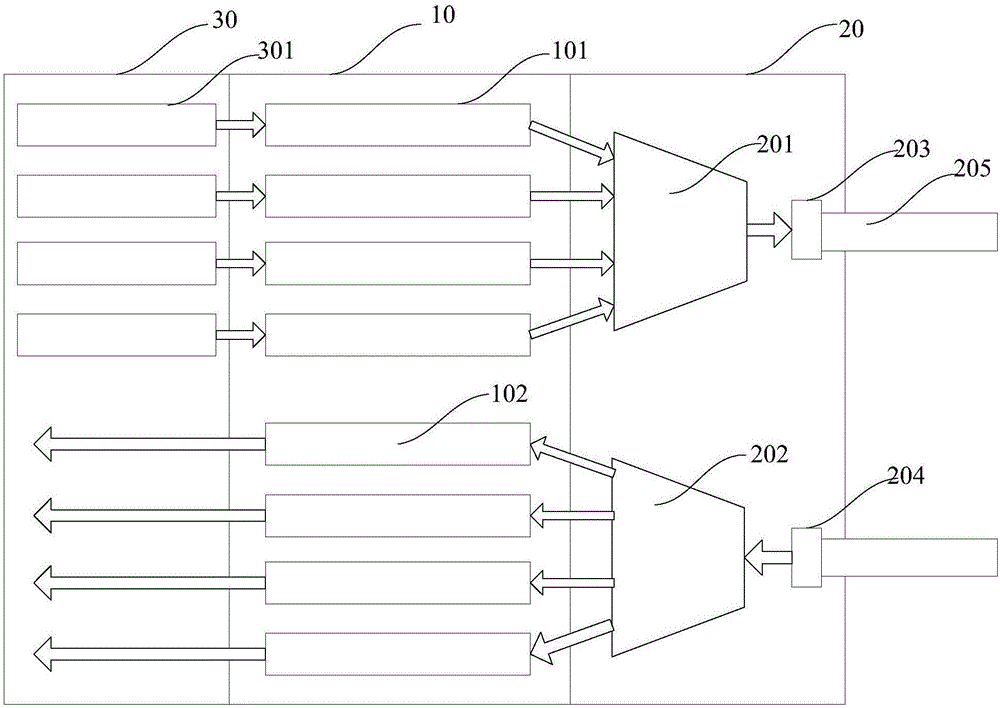
[0044] Such as figure 1 As shown, this embodiment provides a silicon-based WDM optical transceiver module, the silicon-based WDM optical transceiver module includes: a silicon photonic chip 10, including a modulator 101 array and a detector 102 array; A wavelength division multiplexer 201 and a demultiplexer 202, the wavelength division multiplexer 201 and the demultiplexer 202 are integrated on the same planar optical waveguide chip 20, the wavelength division multiplexer 201 and the modulator The array 101 is connected through packaging, and the demultiplexer 202 is connected with the array of detectors 102 through packaging.

[0045] Wavelength division multiplexing technology is a technology that simultaneously transmits multi-wavelength optical signals in one optical fiber. The basic principle is to combine (multiplex) optical signals of different wavelengths through a multiplexer (mux) at the sending end, and couple them to the same optical fiber on the optical cable li...

Embodiment 2

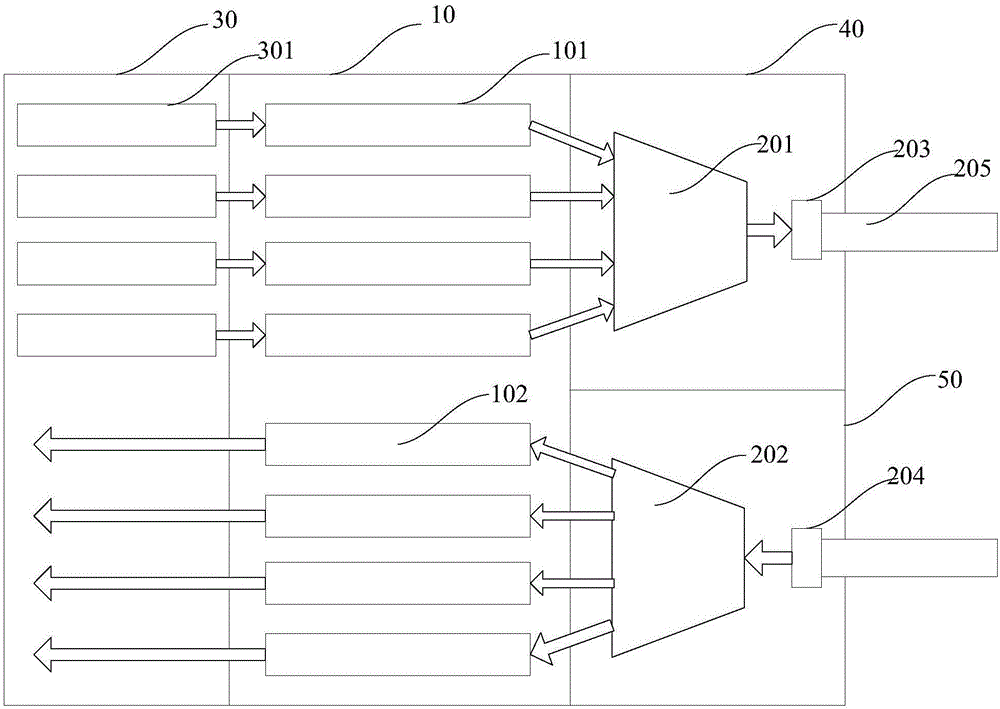
[0056] Such as figure 2 As shown, this embodiment provides a silicon-based WDM optical transceiver module, the silicon-based WDM optical transceiver module includes: a silicon photonic chip 10, including a modulator 101 array and a detector 102 array; A wavelength division multiplexer 201 and a demultiplexer 202, the wavelength division multiplexer 201 and the demultiplexer 202 are planar optical waveguide chips 40 and 50 independently arranged respectively, the wavelength division multiplexer 201 and the demultiplexer 201 The array of modulators 101 is connected through packaging, and the demultiplexer 202 is connected with the array of detectors 102 through packaging. The wavelength division multiplexer 201 and the demultiplexer 202 realized based on planar optical waveguide technology and the silicon photonic chip 10 are independently arranged chips.

[0057] Wavelength division multiplexing technology is a technology that simultaneously transmits multi-wavelength optical...


PUM


Abstract

The invention provides a silicon-based WDM optical transceiver module comprising a silicon photonic chip including a modulator array and a detector array; and a wavelength division multiplexer and a demultiplexer achieved based on a planar lightwave circuit (PLC). The wavelength division multiplexer and the modulator array are connected through packaging. The demultiplexer is connected to the detector array connected through packaging. A WDM optical module is achieved by packaging the wavelength division multiplexer chip and the demultiplexer chip through the silicon photonic chip and the PLC so as to avoid process difficulty of the silicon-based wavelength division multiplexer/demultiplexer. In view of low integration and high power consumption of a traditional WDM optical transceiver module based on discrete devices and PLC, the modulator array and the detector array are integrated by using silicon photon technology so as to greatly improve the integration of optical transceiver module and to reduce power consumption.

Description

technical field [0001] The invention belongs to the field of semiconductors and optoelectronic integration, in particular to a silicon-based WDM optical transceiver module realized by hybrid integration of silicon photonics and PLC. Background technique [0002] With the continuous improvement of people's requirements for information transmission and processing speed and the advent of the era of multi-core computing, metal-based electrical interconnections will become a development bottleneck due to defects such as overheating, delay, and electronic interference. The use of optical interconnection to replace electrical interconnection can effectively solve this problem. In the specific implementation of optical interconnection, silicon-based optical interconnection has become the first choice due to its unparalleled cost and technical advantages. Silicon-based optical interconnection can not only give full play to the advantages of fast optical interconnection speed, large ...

Claims


Application Information

Patent Timeline
Patent Type & Authority Applications(China)
IPC IPC(8): G02B6/42G02B6/43
CPCG02B6/4246G02B6/4204G02B6/43
Inventor 仇超虞婷婷武爱民盛振高腾甘甫烷赵颖璇李军
Owner SHANGHAI INT MICRO TECH AFFILIATION CENT
Why Eureka
Try Eureka