Organic photoelectric device and preparation method thereof and composition with hole transport performance

A technology of photoelectric devices and hole transport layers, which is applied in the manufacture of organic semiconductor devices, electrical solid devices, semiconductor/solid devices, etc., can solve the problems of reduced carrier transport performance, limited large-scale applications, and poor contact performance. Achieve the effect of improving interface contact performance, increasing interface charge transfer efficiency, and low cost

Active Publication Date: 2017-05-10
SHENZHEN UNIV
View PDF5 Cites 17 Cited by
  • Summary
  • Abstract
  • Description
  • Claims
  • Application Information

AI Technical Summary

Problems solved by technology

In addition, the contact between the transition metal oxide nanoparticles prepared by the existing low-temperature solution method is poor, and there are many defects, which will lead to a decrease in the carrier transport performance of the material.
These problems limit its large-scale application
Similar

Method used


Image

  • Organic photoelectric device and preparation method thereof and composition with hole transport performance
  • Organic photoelectric device and preparation method thereof and composition with hole transport performance
  • Organic photoelectric device and preparation method thereof and composition with hole transport performance

Examples


preparation example Construction

[0052] In a second aspect, an embodiment of the present invention provides a method for preparing an organic photoelectric device, including:

[0053] provide the anode;

[0054] Prepare a hole transport layer on the anode by coating or printing, then prepare a functional layer on the hole transport layer, and prepare a cathode on the functional layer to obtain an organic photoelectric device, or

[0055] provide the cathode;

[0056] Prepare a functional layer on the cathode, and then prepare a hole transport layer on the functional layer by coating or printing, and prepare an anode on the hole transport layer to obtain an organic photoelectric device;

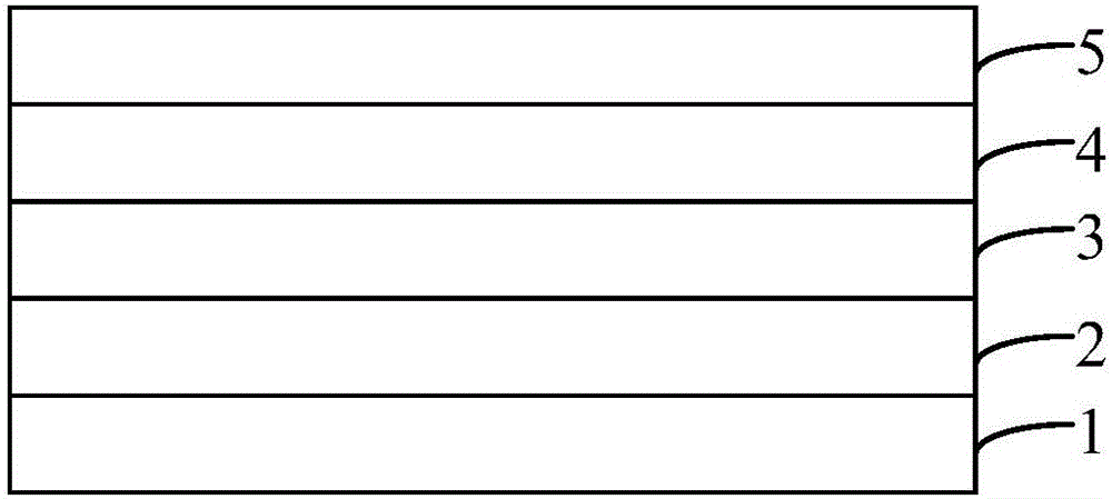
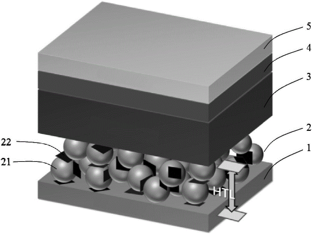
[0057] The functional layer includes a photoelectric active layer or a light-emitting layer, the material of the hole transport layer includes black phosphorus, the number of layers of the black phosphorus is single layer or multiple layers, and the lateral size of the black phosphorus is 1nm-100μm.

[0058] In one embodime...

Embodiment 1

[0105] A method for preparing a composition with hole transport properties, comprising:

[0106] (1) Nanoscale WO 3 Place in isopropanol and centrifuge at 1000 rpm for 4 minutes to remove large particles and take the supernatant to obtain nanoscale WO 3 solution;

[0107] Grind black phosphorus (BP) crystals into powder, add NMP and NaOH, stir vigorously at 10°C for 1 hour, centrifuge at 100rpm for 5 minutes, take the supernatant to obtain a solution containing black phosphorus; the number of layers of black phosphorus is about 20, The lateral dimension of black phosphorus is 100 μm;

[0108] (2) Nanoscale WO 3 The solution is mixed with a solution containing black phosphorus to obtain a mixed solution, and in the mixed solution, nanoscale WO 3 The mass ratio to black phosphorus is 95:5, and the mixed solution is dried to obtain a composition with hole transport properties. Compositions with hole transport properties include black phosphorus and nanoscale WO 3 Particles,...

Embodiment 2

[0110] A method for preparing a composition with hole transport properties, comprising:

[0111] (1) Nanoscale MoO 3 Place in ethanol and centrifuge at 1000 rpm for 4 minutes to remove large particles and take the supernatant to obtain nano-sized MoO 3 solution;

[0112] Grind black phosphorus (BP) crystals into powder, add NMP and NaOH, stir vigorously at 50°C for 10 hours, centrifuge at 7000rpm for 20 minutes, take the supernatant to obtain a solution containing black phosphorus; the number of layers of black phosphorus is about 10 , the lateral dimension of black phosphorus is 10 μm;

[0113] (2) Nanoscale MoO 3 The solution is mixed with a solution containing black phosphorus to obtain a mixed solution, and in the mixed solution, nanoscale MoO 3 The mass ratio to black phosphorus is 90:10, the mixed solution is ultrasonically reacted at 70° C. for 40 min, and the obtained product is dried to obtain a composition with hole transport properties. Compositions with hole-t...


PUM

PropertyMeasurementUnit
Horizontal sizeaaaaaaaaaa

Abstract

The invention provides an organic photoelectric device, which comprises an anode, a functional layer, a cathode and a hole transport layer located between the anode and the functional layer, wherein the functional layer comprises a photoelectric active layer or a light-emitting layer; the material of the hole transport layer comprises black phosphorus; the black phosphorus is single-layer or multi-layer; and the transverse size of the black phosphorus is 1nn to 100 microns. According to the organic photoelectric device, the interfacial charge transfer efficiency and the hole mobility of a bulk phase can be improved, thereby effectively improving the performance of the device. The invention further provides a preparation method of the organic photoelectric device. The method comprises the steps of providing the anode; preparing the hole transport layer on the anode by adopting a coating or printing method and then preparing the functional layer on the hole transport layer; and preparing the cathode on the functional layer to obtain the organic photoelectric device; or providing the cathode; preparing the functional layer on the cathode and then preparing the hole transport layer on the functional layer adopting the coating or printing method; and preparing the anode on the hole transport layer to obtain the organic photoelectric device. The preparation method is simple and easy to operate.

Description

technical field [0001] The invention relates to the technical field of organic photoelectric devices, in particular to an organic photoelectric device, a preparation method thereof, and a composition with hole transport properties. Background technique [0002] Organic optoelectronic devices include organic electroluminescent devices (OLEDs) and organic solar cells (OSCs). Generally, organic optoelectronic devices include multiple layers of materials, such as hole transport layers. Taking organic solar cells as an example, in organic solar cells, the lifetime of electrons generated after electron-hole separation is extremely short (only tens of femtoseconds), if If electrons cannot be collected by the electrodes in time, they are easy to recombine with holes, which reduces the energy conversion efficiency of the battery device; and there are many defects on the surface of the photoelectric active layer and there is a large potential barrier between the metal electrode and it...

Claims


Application Information

Patent Timeline
IPC IPC(8): H01L51/42H01L51/48H01L51/50H01L51/56B82Y30/00
CPCB82Y30/00H10K71/12H10K30/15H10K50/155H10K2102/00H10K71/00Y02E10/549
Inventor 张晗仇萌张家宜
Owner SHENZHEN UNIV
Why Eureka
Try Eureka