A kind of manufacturing method of light-emitting diode epitaxial wafer

A technology of light-emitting diodes and manufacturing methods, which is applied to semiconductor devices, electrical components, circuits, etc., can solve the problems of large energy band bending, enhanced polarization effect, and small carrier confinement, so as to improve crystal quality and reduce V type dislocation and linear dislocation, reducing the effect of polarization effect

Active Publication Date: 2019-03-08
HC SEMITEK ZHEJIANG CO LTD
View PDF5 Cites 0 Cited by
  • Summary
  • Abstract
  • Description
  • Claims
  • Application Information

AI Technical Summary

Problems solved by technology

[0005] InGaN, GaN, and AlGaN have stresses due to the lattice mismatch. The stress makes the polarization effect of the multi-quantum well layer stronger, the energy band bends greatly, and the binding effect on the carriers is small, which affects the internal quantum efficiency of the LED. and antistatic properties

Method used


Image

  • A kind of manufacturing method of light-emitting diode epitaxial wafer
  • A kind of manufacturing method of light-emitting diode epitaxial wafer
  • A kind of manufacturing method of light-emitting diode epitaxial wafer

Examples


Embodiment

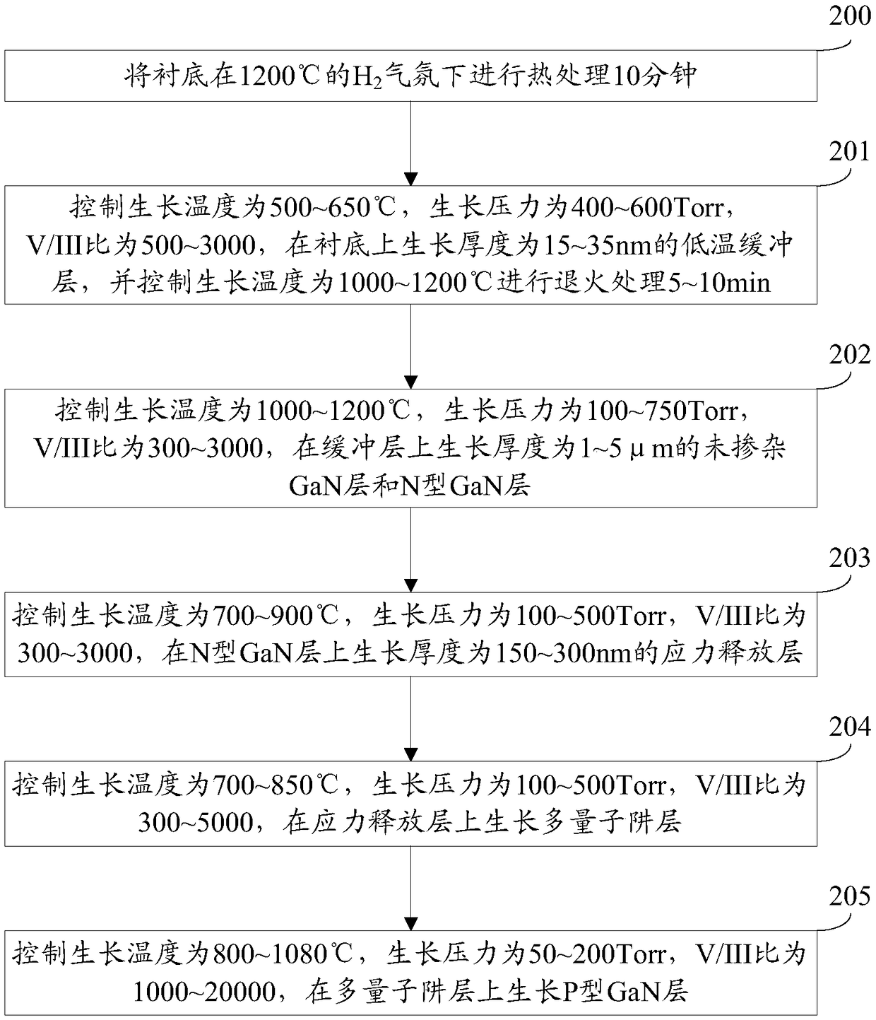
[0027] The embodiment of the present invention provides a method for manufacturing a light-emitting diode epitaxial wafer, using high-purity hydrogen (H 2 ) or nitrogen (N 2 ) as carrier gas, trimethylgallium (TMGa), trimethylaluminum (TMAl), trimethylindium (TMIn) and ammonia (NH 3 ) as Ga, Al, In and N sources respectively, with silane (SiH 4 ), Magnesium (Cp 2 Mg) as N and P type dopants respectively. see figure 1 , the manufacturing method includes:

[0028] Step 200: Put the substrate at 1200°C in H 2 The heat treatment was performed for 10 minutes under the atmosphere.

[0029] In this embodiment, the substrate can be sapphire, Si or SiC.

[0030] It should be noted that heat treatment can clean the surface of the substrate.

[0031] Step 201: Control the growth temperature to 500-650° C., the growth pressure to 400-600 Torr, and the V / III ratio to 500-3000, grow a low-temperature buffer layer with a thickness of 15-35 nm on the substrate, and control the growth ...


PUM

PropertyMeasurementUnit
thicknessaaaaaaaaaa
temperatureaaaaaaaaaa
thicknessaaaaaaaaaa

Abstract

The invention discloses a manufacturing method of a light-emitting-diode epitaxial wafer and belongs to the semiconductor technology field. The manufacturing method comprises the following steps that a low temperature buffer layer, a un-doped GaN layer, an N type GaN layer, a stress release layer, a multi-quantum well layer and a P type GaN layer are successively grown on a substrate, wherein the stress release layer includes an InGaN layer and an AlxGaN layer which are alternatively stacked, and the x is greater than or equal to 0 and is less than 0.3; and during a growing process of the AlxGaN layer, a growth temperature of the AlxGaN layer reaches a maximum temperature from a growth temperature of the InGaN layer through several stages of heating and then reaches the growth temperature of the InGaN layer from the maximum temperature through several stages of cooling, and the temperature in a same stage is constant and the temperatures of the two adjacent stages are different. In the invention, through slow changes of the temperature, a stress in a gallium nitride layer is fully released, a polarized effect is reduced, V-shaped dislocation and linear dislocation in the epitaxial layer are decreased, and crystal quality is increased.

Description

technical field [0001] The invention relates to the technical field of semiconductors, in particular to a method for manufacturing a light-emitting diode epitaxial wafer. Background technique [0002] GaN-based light-emitting diodes (English: Lighting Emitting Diode, referred to as LED) have the characteristics of small size, long service life, colorful colors, and low energy consumption. They are widely used in outdoor full-color displays, traffic lights, backlights, etc. , is considered to be one of the options most likely to replace incandescent and fluorescent lamps in the future. [0003] LED epitaxial wafers usually include a substrate, and a low-temperature buffer layer, an undoped GaN layer, an N-type GaN layer, a multi-quantum well layer, and a P-type GaN layer stacked on the substrate in sequence. Wherein, the multi-quantum well layer includes alternately stacked quantum well layers and quantum barrier layers, the quantum well layer is an InGaN layer, and the quan...

Claims


Application Information

Patent Timeline
Patent Type & Authority Patents(China)
IPC IPC(8): H01L33/32H01L33/06H01L33/02H01L33/00
CPCH01L33/005H01L33/02H01L33/06H01L33/32
Inventor 武艳萍
Owner HC SEMITEK ZHEJIANG CO LTD
Why Eureka
Try Eureka