Silicon-based inverted microstrip line structure and manufacturing method therefor

A technology of inverting microstrip and line structures, applied in the direction of microstructure technology, microstructure devices, manufacturing microstructure devices, etc., can solve problems such as difficult accuracy, dielectric loss, and limited applications, so as to reduce the emission of secondary electrons, reduce the Small insertion loss and simple manufacturing method

Active Publication Date: 2017-05-17
XIDIAN UNIV
View PDF2 Cites 3 Cited by
  • Summary
  • Abstract
  • Description
  • Claims
  • Application Information

AI Technical Summary

Problems solved by technology

[0003] However, since the traditional inverted microstrip line has a thicker dielectric substrate as the inversion layer to fix the microstrip line, the dielectric substrate will bring significant dielectric loss when transmitting millimeter-wave and submillimeter electromagnetic energy, which limits the ability of the inverted microstrip line. The scope of use of the belt
In addition, the traditional inverted microstrip line also needs a metal box as a metal shielding cavity, which has high cost, large volume, high quality, and low precision, and the small-sized standard microstrip line structure is difficult to achieve high-precision processing.
Traditional inverted microstrip lines generally use microwave boards, plastics, ceramics and other materials as dielectric substrates for fixing microstrip lines, but microwave boards are difficult to process into thin-layer support structures, and plastics and ceramics are not easy to achieve sub-μm precision. The preparation of the traditional suspended microstrip line cannot be compatible with the traditional IC process. In addition, when the operating frequency reaches the terahertz frequency band, it is difficult for the ordinary processing technology to realize the small-sized high-precision structure of the transmission line. These factors not only affect the performance of the traditional inverted microstrip line and reliability, and limit its application in portable or highly integrated products

Method used


Image

  • Silicon-based inverted microstrip line structure and manufacturing method therefor
  • Silicon-based inverted microstrip line structure and manufacturing method therefor
  • Silicon-based inverted microstrip line structure and manufacturing method therefor

Examples


Embodiment Construction

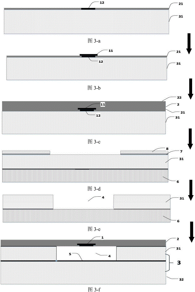
[0051]The present invention will be described in further detail below in conjunction with the accompanying drawings. Described embodiment is only a part of embodiment of the present invention, not all embodiment, the present invention can also adopt other different modes to implement, those skilled in the art can do similar promotion under the situation of not violating connotation of the present invention, Therefore, the present invention is not limited by the specific examples disclosed below.

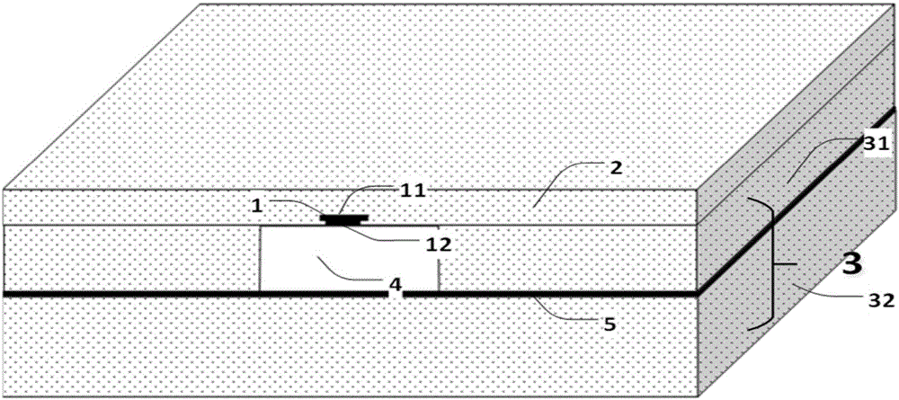
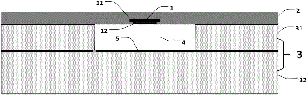
[0052] see figure 1 , 2. The silicon-based inverted microstrip line structure of the present invention includes a lower silicon substrate 32 , an upper silicon substrate 31 and an inversion layer 2 arranged in sequence from bottom to top. The inversion layer 2 is prepared by using SU8 photoresist, and its thickness is between 10 μm and 20 μm. The upper silicon substrate 31 is made of 110 silicon, the width of the upper metal layer 11 is 1.2 to 1.4 times that of the lower metal laye...


PUM

PropertyMeasurementUnit
thicknessaaaaaaaaaa
thicknessaaaaaaaaaa

Abstract

The invention discloses a silicon-based inverted microstrip line structure and a manufacturing method therefor, and mainly solves the problems of high loss and low processing precision in millimeter wave and submillimeter wave transmission by a standard microstrip line and a conventional inverted microstrip line. The silicon-based inverted microstrip line structure comprises a microstrip line, a suspension layer, a silicon substrate, a cavity and a metal grounding layer, wherein the silicon substrate comprises an upper silicon substrate and a lower silicon substrate; and inverted layer is positioned on the upper surface of the upper silicon substrate; the microstrip line comprises a lower metal layer and an upper metal layer; the upper metal layer is fixed in the inverted layer; the lower metal layer is prepared on the lower surface of the upper metal layer and exposed in the cavity; the cavity is formed in the upper silicon substrate in an etching manner, positioned below the microstrip line and suspends the microstrip line; and the metal grounding layer is positioned below the cavity and embedded between the upper silicon substrate and the lower silicon substrate. The manufacturing method is high in processing precision, and a low-loss and simple-manufacturing millimeter wave transmission line structure is realized.

Description

technical field [0001] The invention belongs to the field of microelectromechanical systems, and in particular relates to a silicon-based inverted microstrip line structure and a manufacturing method thereof. Background technique [0002] Micromechanical electronic systems (MEMS) are developed on the basis of microelectronics technology, and are often used to process microstructures to achieve anisotropic etching. MEMS technology usually uses silicon wafers or SOI as substrates, uses sub-μm precision masks prepared by microelectronics technology to precisely define the size of graphics, and uses special masks to achieve high aspect ratio etching of bulk structures. The commonly used deep etching methods include dry etching and wet etching. Among them, dry etching generally does not depend on the crystal orientation, but the processing complexity is high, and expensive etching equipment needs to be used; wet etching Etching uses the sensitivity of different crystal orientati...

Claims


Application Information

Patent Timeline
Patent Type & Authority Applications(China)
IPC IPC(8): H01P3/08B81C1/00B81B7/02
CPCB81B7/02B81C1/00015H01P3/08H01P3/081
Inventor 吕玲王少波杜林马晓华张进成曹艳荣习鹤郝跃
Owner XIDIAN UNIV
Why Eureka
Try Eureka