
An on-chip integrated optical power beam splitter based on silicon-based metamaterials

An integrated optical and metamaterial technology, applied in instruments, optics, light guides, etc., can solve the problems of poor wavelength independence and small size, and achieve the effect of reducing insertion loss, facilitating on-chip integration, and compact structure

Active Publication Date: 2019-10-18
BEIJING UNIV OF POSTS & TELECOMM
View PDF7 Cites 0 Cited by
  • Summary
  • Abstract
  • Description
  • Claims
  • Application Information

AI Technical Summary

Problems solved by technology

[0009] For the directional coupler (DC), due to the characteristics of its structure, its size cannot be made small, and its wavelength independence is poor

Method used


Image

  • An on-chip integrated optical power beam splitter based on silicon-based metamaterials
  • An on-chip integrated optical power beam splitter based on silicon-based metamaterials
  • An on-chip integrated optical power beam splitter based on silicon-based metamaterials

Examples


Embodiment Construction

[0024] The present invention will be further described in detail with reference to the accompanying drawings and implementation examples.

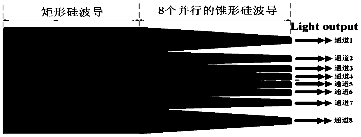
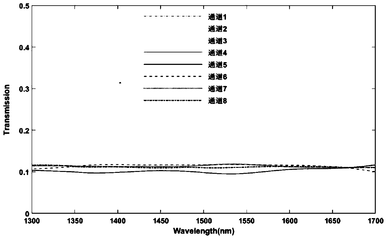
[0025] The invention relates to an on-chip integrated optical power beam splitter based on a silicon-based metamaterial, which is used to realize equal power beam splitting of super multi-path light. Such as figure 1 As shown, it includes a rectangular silicon waveguide and 8 parallel tapered silicon waveguides. The specific implementation is to cut the second half of the entire rectangular silicon waveguide into 8 tapered shapes with different widths according to the size ratio. The refractive index of the entire silicon waveguide is 3.46; The length*width*height dimensions of the uncut rectangular silicon waveguide are: 10um*12um*0.22um, used as the input port, and 8 parallel tapered silicon waveguides cut in parallel are used as the output port.

[0026] The tapered silicon waveguide is a horizontal trapezoid on the xy plane, the width...


PUM


Abstract

The invention discloses an on-chip integrated optical power splitter based on silicon-based metamaterial and belongs to the technical field of on-chip integrated silicon photonics. The on-chip integrated optical power splitter based on silicon-based metamaterial comprises a rectangular silicon waveguide and N parallel conical silicon waveguides connected to the same seamlessly in series; the rectangular silicon waveguide serves as an optical input port; the N conical silicon waveguides serve as output ports and are symmetric about X axis; N channels are equal in both length and height, the width of each channel is determined according to proportional distribution of optical field strength in cross-section yz direction, and every two symmetric channels are equal in size; with the channels increasing in number, only longitudinal size in the width direction of the silicon waveguides increases, while the transverse size in the length direction of the silicon waveguides is substantially unchanged; according to optical field distribution, strength distribution proportion of an optical field is width proportional size of the N silicon waveguides. The on-chip integrated optical power splitter based on silicon-based metamaterial is compact in structure and simple in design, has reduced device insert loss at smaller size, and allows equal optical power distribution for any number of channels.

Description

technical field [0001] The invention belongs to the technical field of on-chip integrated silicon photonics, relates to an optical waveguide device, and specifically refers to an on-chip integrated optical power beam splitter based on a silicon-based metamaterial. Background technique [0002] In recent years, various Internet services have emerged, especially with the continuous rise of new technologies such as cloud storage, cloud computing and big data, and global information exchange has shown explosive growth. While information exchange is becoming more and more convenient, the requirements for high-speed and large-capacity communication systems are also getting higher and higher. In view of the increasingly prominent bottleneck effect of electronic carriers, optical interconnection technology has gradually become the mainstream technology to overcome the bottleneck of communication network transmission. [0003] As the core of optical interconnect technology, integrat...

Claims


Application Information

Patent Timeline
Patent Type & Authority Patents(China)
IPC IPC(8): G02B6/12G02B6/122
Inventor 杨大全王波陈鑫纪越峰
Owner BEIJING UNIV OF POSTS & TELECOMM
Learn More