Large-area nanometer slot array and manufacturing method therefor

A nano-gap, large-area technology, applied in the direction of photolithography process exposure devices, microlithography exposure equipment, etc., can solve the problems of complex process, limited nano-gap preparation efficiency, and difficulty in making templates for nano-imprinting, and achieves the cost of the process. wide range of effects

Inactive Publication Date: 2017-05-31
SICHUAN UNIV
View PDF4 Cites 9 Cited by
  • Summary
  • Abstract
  • Description
  • Claims
  • Application Information

AI Technical Summary

Problems solved by technology

However, their disadvantages are as significant as their advantages, that is, they are not only costly and complicated, but also cannot be fabricated in a large area, which greatly limits the efficiency of nanoslit preparation.
Nanoimprinting is also a commonly used method of micro-nano processing, but it is difficult to make templates for nanoimprinting
Extreme ultraviolet lithography has fast manufacturing speed and high resolution, but requires a higher extreme ultraviolet light source
The laser lithography system has the advantages of stable performance, low cost, and convenient use, but the resolution is relatively low

Method used


Image

  • Large-area nanometer slot array and manufacturing method therefor
  • Large-area nanometer slot array and manufacturing method therefor
  • Large-area nanometer slot array and manufacturing method therefor

Examples


Embodiment Construction

[0018] The following describes in detail the embodiments of the present invention that are used to make large-area nanoslit array structures. To further describe the present invention, it is necessary to point out that the following embodiments are only used for further description of the present invention and cannot be interpreted as protecting the present invention. Limitation of the scope, some non-essential improvements and adjustments to the present invention by those skilled in the art according to the above content of the invention still belong to the protection scope of the present invention.

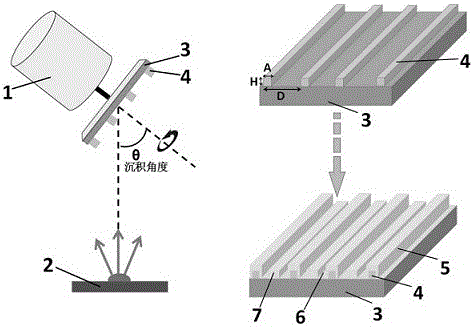
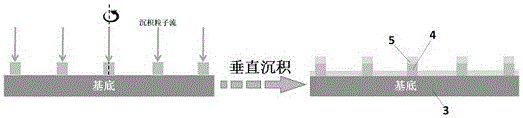
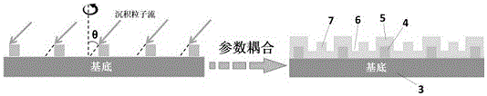
[0019] The steps of interference laser lithography include depositing adhesive on the surface of the silicon wafer, spin-coating photoresist, pre-baking, performing interference exposure in the interference lithography system, and then developing, by controlling the exposure time and development time To adjust the duty cycle of the grating.

[0020] One embodiment of the present...


PUM


Abstract

The invention discloses a manufacturing method for a large-area nanometer slot array, and relates to the field of micro-nano machining. By combination of an angle deposition shadow effect and substrate rotation, and by regulating a rotary speed of the substrate, a nanometer mask structure, a deposition angle and a deposition speed parameter to be matched mutually, the novel and large-area nanometer slot array is manufactured. In addition, based on the technology disclosed by the invention and by taking a raster as a deposition mask substrate, a large-area periodical nanometer slot array structure is already manufactured.

Description

technical field [0001] The invention relates to the field of micro-nano processing, in particular to a method for manufacturing a large-area nano-slit array structure. Background technique [0002] The nanoscale gap structure has a wide range of applications in the fields of optics, nanoelectronic devices, and biomedical detection. Due to the electromagnetic coupling of metal nanoslits, the electric field on the surface of the structure is greatly enhanced, which can also be used to enhance fluorescence and Raman scattering. Therefore, it is urgent to develop a new technology that can accurately and large-area fabricate nanoslit structures. [0003] The technical route of nanotechnology research can be divided into two processing methods: "top-down" and "bottom-up". At present, the main methods commonly used to fabricate nanoslits include electron beam lithography, ion beam lithography, nanoimprinting, extreme ultraviolet lithography, and laser lithography. Among them, el...

Claims


Application Information

Patent Timeline
Patent Type & Authority Applications(China)
IPC IPC(8): G03F7/20
CPCG03F7/70
Inventor 时元振庞霖
Owner SICHUAN UNIV
Why Eureka
Try Eureka