Organic light-emitting device and manufacturing method thereof

An electroluminescent device and luminescence technology, which is applied in the direction of electric solid-state devices, semiconductor/solid-state device manufacturing, electrical components, etc., can solve the problems of low luminous efficiency, high cost, and light loss of devices, and achieve improved front luminous intensity, Enhanced electrical conductivity and improved light extraction efficiency

Inactive Publication Date: 2013-10-30
OCEANS KING LIGHTING SCI&TECH CO LTD +1
View PDF9 Cites 0 Cited by
  • Summary
  • Abstract
  • Description
  • Claims
  • Application Information

AI Technical Summary

Problems solved by technology

[0004] In traditional electroluminescent devices, the most researched is the bottom-emitting device structure, with the ITO glass substrate as the light-emitting surface. This kind of device has mature technology and has been studied a lot. Because the light will first go through the absorption and reflection of the ITO conductive material. , it needs to be absorbed and reflected by the glass again, and finally it can be emitted into the air. Since the glass surface is relatively flat and the glass thickness is relatively large, the optical path is increased, so that more light is refracted to both sides of the glass. The probability of light emitted from the glass to the device is reduced, which ultimately affects the luminous efficiency. Therefore, the emission rate of light emitted into the air is very low, and most of the light is lost. The luminous efficiency of this type of device is low.
Moreover, ITO is expensive, and the indium tin components in it are rare metals, and the output is very small, which is not suitable for mass production of products

Method used


Image

  • Organic light-emitting device and manufacturing method thereof
  • Organic light-emitting device and manufacturing method thereof

Examples


preparation example Construction

[0039] The preparation method of the above-mentioned laminated organic electroluminescent device comprises the following steps:

[0040] S1. Clean the glass substrate sequentially with detergent, deionized water, acetone, ethanol, and isopropanol for 15 minutes to remove organic pollutants on the glass surface

[0041] S2. Using an evaporation process, evaporating a metal layer with a thickness of 5-20 nm on the surface of the cleaned glass substrate;

[0042] S3. Using a spin coating process, spin coating an activated carbon suspension solution on the surface of the metal layer to prepare an activated carbon layer with a thickness of 1-100 μm;

[0043] S4, using the evaporation process again, sequentially stacking the evaporation hole transport layer, light emitting layer, electron transport layer, electron injection layer and cathode layer on the surface of the activated carbon layer;

[0044] After the process steps are completed, the organic electroluminescent device is p...

Embodiment 1

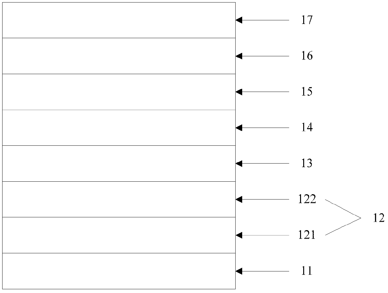
[0053] The organic electroluminescent device structure of the present embodiment: glass / (Ag / activated carbon) / TCTA / TPBi:Ir(ppy) 3 / TAZ / LiF / Ag.

[0054] The preparation process of the organic electroluminescent device is as follows:

[0055] Firstly, ultrasonically clean the glass substrate with detergent, deionized water, acetone, ethanol, and isopropanol for 15 minutes each to remove organic pollutants on the glass surface;

[0056] Evaporate metal layer (material is Ag, thickness is 10nm) on the glass substrate surface after cleaning; Then spin-coat active carbon suspension solution (the mass percentage of active carbon is 20%) on the surface of metal layer, make the active carbon layer that thickness is 10 μm ;

[0057] Then on the surface of the activated carbon layer, the vapor-deposited hole transport layer (the material is TCTA with a thickness of 50nm), the light-emitting layer (the material is TPBi:Ir(ppy) 3 , ie Ir(ppy) 3 Doped into TPBi, and Ir(ppy) 3 Doping ma...

Embodiment 2

[0060] The organic electroluminescent device structure of the present embodiment: glass / (Al / activated carbon) / TCTA / TPBi:Ir(MDQ) 2 (acac) / Bphen / Cs 2 CO 3 / Au.

[0061] The preparation process of the organic electroluminescent device is as follows:

[0062] Firstly, ultrasonically clean the glass substrate with detergent, deionized water, acetone, ethanol, and isopropanol for 15 minutes each to remove organic pollutants on the glass surface;

[0063] Evaporate metal layer (material is Al, thickness is 5nm) on the glass substrate surface after cleaning; Then spin-coat activated carbon suspension solution (the mass percent of activated carbon is 5.21%) on the surface of metal layer, the activated carbon layer that makes thickness is 1 μm ;

[0064] Subsequently, on the surface of the activated carbon layer, the vapor-deposited hole transport layer (the material is TCTA with a thickness of 60nm), the light-emitting layer (the material is TPBi:Ir(MDQ) 2 (acac), ie Ir(MDQ) 2 (a...


PUM


Abstract

The invention belongs to the field of organic light-emitting devices and discloses an organic light-emitting device and a manufacturing method thereof. The organic light-emitting device comprises a glass substrate, a conductive anode layer, a hole transmission layer, a luminous layer, an electron transmission layer, an electron injection layer and a cathode layer, wherein the glass substrate, the conductive anode layer, the hole transmission layer, the luminous layer, the electron transmission layer, the electron injection layer and the cathode layer are stacked sequentially, the conductive anode layer comprises a metal layer and an activated carbon layer, the metal layer is stacked on the surface of the glass substrate, and the activated carbon layer is stacked on the surface of the metal layer. According to the organic light-emitting device, a mixed material of activated carbon suspension liquid and metal replaces ITO to be used as the anode of the organic light-emitting device, activated carbon can enhance the electrical conductivity of the organic light-emitting device and can further enhance the scattering of light, the incident angle of the light on a glass surface is changed, the probability of total reflection of the light is reduced, the light extraction rate and the front light-emitting strength are improved, and meanwhile the activated carbon is low in price, non-toxic and free of pollution.

Description

technical field [0001] The invention relates to the field of electroluminescent devices, in particular to an organic electroluminescent device and a preparation method thereof. Background technique [0002] In 1987, C.W.Tang and Van Slyke of Eastman Kodak Company in the United States reported a breakthrough in the research of organic electroluminescence. A high-brightness, high-efficiency double-layer organic electroluminescent device (OLED) was prepared by using ultra-thin film technology. In this double-layer structure device, the brightness reaches 1000cd / m at 10V 2 , its luminous efficiency is 1.51lm / W, and its lifespan is more than 100 hours. [0003] The principle of OLED light emission is based on the action of an external electric field, electrons are injected from the cathode to the lowest unoccupied molecular orbital (LUMO) of organic matter, and holes are injected from the anode to the highest occupied orbital (HOMO) of organic matter. Electrons and holes meet,...

Claims


Application Information

Patent Timeline
Patent Type & Authority Applications(China)
IPC IPC(8): H01L51/52H01L51/50H01L51/56
Inventor 周明杰王平黄辉陈吉星
Owner OCEANS KING LIGHTING SCI&TECH CO LTD
Why Eureka
Try Eureka