Multifunctional and multilayer-plate type array voltage dependent resistor and preparation method of multifunctional and multilayer-plate type array voltage dependent resistor
A technology of varistors and multi-layer boards, applied in varistors, thin film varistors, resistors, etc., can solve problems such as poor noise absorption performance, affecting product use, slow response speed, etc., and achieve impact resistance and Strong vibration ability, improve the ability to resist electromagnetic interference, and ensure the effect of quality and reliability
- Summary
- Abstract
- Description
- Claims
- Application Information
AI Technical Summary
Problems solved by technology
Method used
Image
Examples
Embodiment 1
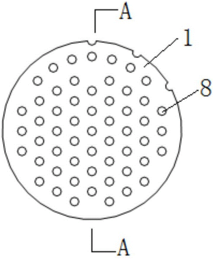
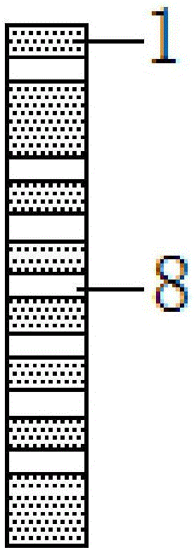
[0047] Such as Figure 1-4 As shown, in order to solve the problems existing in the prior art, the present invention provides a multifunctional multilayer plate array varistor, including: a resistor body 1, a ceramic diaphragm 2, a common ground electrode 3, a signal electrode 4, Ground terminal 5, signal terminal 6, surface coating layer 7 and signal hole 8;
[0048] The resistor body 1 of the present invention is an annular ceramic plate with a plurality of signal holes 8, and the axis of the signal hole 8 is parallel to the axis of the ceramic plate, as Figure 1-2 Shown; Resistor main body 1 of the present invention can also be set to other shapes, and resistor main body 1 is made of multilayer ceramic diaphragm 2 and inner electrode; Wherein:
[0049]The ceramic diaphragm 2 of the present invention does not perform arc treatment on the corners and edges, the thickness of the ceramic diaphragm 2 is 50um to 200um, and the ceramic diaphragm 2 is a sheet-like structure made ...
Embodiment 2
[0056] The invention provides a method for preparing a multifunctional multilayer plate array piezoresistor, comprising:
[0057] Step 1, preparing green chips by wet printing or casting;
[0058] Step 2, plasticizing and sintering the green chip to prepare the main body of the resistor;
[0059] Step 3. Prepare the ground terminal, the signal terminal and the surface coating layer on the main body of the resistor to complete the preparation of the multifunctional multi-layer plate array piezoresistor.
[0060] Among them, the present invention is the same as the existing stacked devices, by using wet printing or casting method to prepare the green chip, by using the die stamping method or laser forming method to process the raw material into a chip with a signal hole according to the required pattern size The green body is plastic-expelled and sintered, and the external electrodes are manufactured by printing or transfer printing and sintering. The following is a detailed d...
Embodiment 3
[0077] Such as Figure 1-4 As shown, the piezoresistor array of the present invention is circular in shape, with a diameter of 20.95mm and a thickness of 3.00mm. The number of layers of the internal electrode is 8 layers, the thickness of the two end layers (the uppermost layer / lower ceramic membrane plate) is 1000 μm, and the thickness of the middle layer (middle layer ceramic membrane plate) is uniform and 120 μm; the metal electrodes are built in two layers of ceramic substrates Between; the signal holes are independent of each other, the signal hole spacing adopts the standard density of 2.54mm, the lead-out is a circular pin lead, the hole diameter is 0.95mm, and the number of planar array contacts is 55; the signal pole lead-out is located on the ceramic plate The inner surface of the small hole in the inner surface; the ground electrode lead-out end is located on the outer surface of the ceramic plate, and the ground electrode lead-out end adopts an uninterrupted multi-...
PUM
 Abstract
Description
Claims
Application Information


