Manufacturing method of three-dimensional bonding stack interconnect integration for radio-frequency microsystem device

A manufacturing method and micro-system technology, applied in semiconductor/solid-state device manufacturing, electric solid-state devices, semiconductor devices, etc., can solve problems such as the inability of precision and volume to meet new requirements, reduce the length of signal lines, and have strong operability , the effect of improving the transmission quality

Inactive Publication Date: 2017-05-31
NO 55 INST CHINA ELECTRONIC SCI & TECHNOLOGYGROUP CO LTD
View PDF5 Cites 22 Cited by
  • Summary
  • Abstract
  • Description
  • Claims
  • Application Information

AI Technical Summary

Problems solved by technology

The LTCC microwave multi-layer substrate double-sided micro-assembly technology is adopted to increase the assembly density. Through the use of high-precision chip mounting technology and chip gold wire bonding technology, the double-sided high-precision chip mounting and gold wire bonding of LTCC microwave multi-layer substrates are realized. Bonding improves the assembly density of microwave components, but the accuracy and volume of MCM technology compared with semiconductor processes cannot meet the new requirements

Method used


Image

  • Manufacturing method of three-dimensional bonding stack interconnect integration for radio-frequency microsystem device
  • Manufacturing method of three-dimensional bonding stack interconnect integration for radio-frequency microsystem device
  • Manufacturing method of three-dimensional bonding stack interconnect integration for radio-frequency microsystem device

Examples


Embodiment Construction

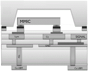
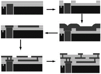
[0022] The integrated manufacturing method for three-dimensional bonded stacked interconnection for radio frequency microsystem devices is characterized in that it includes the following steps:

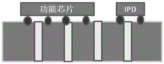
[0023] 1) Realize the three-dimensional integration of RF microsystem devices through chip-to-wafer bonding, wafer-to-wafer bonding, and multi-layer dielectric-metal alternate wiring, including at least adding three layers of heterogeneous devices to traditional silicon-based planar devices , material or cap;

[0024] 2) High-resistance silicon is used as the substrate or adapter board; the substrate or adapter board is alternately completed with multi-layer dielectric-metal wiring for radio frequency signal transmission and control;

[0025] 3) The heterogeneous compound chip is integrated through chip to wafer bonding;

[0026] 4) All chips are connected to the silicon substrate or the metal bump on the adapter board through the bottom pad to realize signal transmission between dif...


PUM


Abstract

The invention provides a manufacturing method of a three-dimensional bonding stack interconnect integration for a radio-frequency microsystem device. The method comprises the steps as follows: high-resistivity silicon is taken as a substrate or an adapter plate; multi-layer dielectric-metal alternate wiring is completed for radio-frequency signal transmission and control on the substrate or the adapter plate; heterogeneous compound chips achieve heterogeneous integration through chip to wafer bonding, all chips are connected with metal bumps on the silicon substrate or the adapter plate through a bottom bonding pad to achieve signal transmission among different layers, and three-layer structure stacking and chip protection are achieved through bonding of wafers with silicon cavities and the wafer of the silicon substrate or the adapter plate; and leading-out of signals of a whole device is achieved by adopting a through-silicon via technology. The method has the advantages that the heterogeneous chips are integrated together through three-layer stacking, so that the original function of the device is greatly improved, leading-out of the signals from bonding interfaces is achieved by adopting the through-silicon via technology, a closed and compact chip structure is formed, three-dimensional heterogeneous integration of a radio-frequency device is really achieved, the technology is simplified, packaging is low in cost and the yield is high.

Description

technical field [0001] The invention relates to a three-dimensional bonding and stacking interconnection integrated manufacturing method for radio frequency microsystem devices, which belongs to the technical field of semiconductors. Background technique [0002] In the three-dimensional bonding stacking interconnection integration process manufacturing method of radio frequency microsystem devices, the three-dimensional integration of multi-layer chips mainly depends on the realization of bonding technology. Through bonding, multi-layer chips can be integrated in the thickness direction, and through-silicon via technology can be used to provide electrical interconnection between different layers of chips to realize three-dimensional integration. Therefore, bonding is an essential process for 3D integration. The introduction of bonding technology not only enables the successful implementation of parallel manufacturing technology solutions in 3D integration to improve product...

Claims


Application Information

Patent Timeline
Patent Type & Authority Applications(China)
IPC IPC(8): H01L27/04H01L23/48H01L21/822H01L21/60
CPCH01L21/822H01L23/481H01L24/10H01L24/11H01L27/04
Inventor 石归雄黄旼吴璟朱健郁元卫
Owner NO 55 INST CHINA ELECTRONIC SCI & TECHNOLOGYGROUP CO LTD
Why Eureka
Try Eureka