Preparing method for large-area metal nanometer needle-tip array on flexible substrate

A large-area metal and flexible substrate technology, applied in the field of nanotechnology, to achieve good performance, expand the application range, and reduce the cost of preparation

Active Publication Date: 2017-06-09
CHINA ELECTRONIC TECH GRP CORP NO 38 RES INST
View PDF5 Cites 16 Cited by
  • Summary
  • Abstract
  • Description
  • Claims
  • Application Information

AI Technical Summary

Problems solved by technology

[0003] The existing micro-nano processing technology has relatively mature process parameters for the preparation of nano-tips with silicon structures, but there are still many difficulties in the processing of nano-tips made of metal materials at the micro-nano scale, so large-scale, low-cost metal The preparation of nano needle tips is one of the important research directions currently existing

Method used


Image

  • Preparing method for large-area metal nanometer needle-tip array on flexible substrate
  • Preparing method for large-area metal nanometer needle-tip array on flexible substrate
  • Preparing method for large-area metal nanometer needle-tip array on flexible substrate

Examples


Embodiment 1

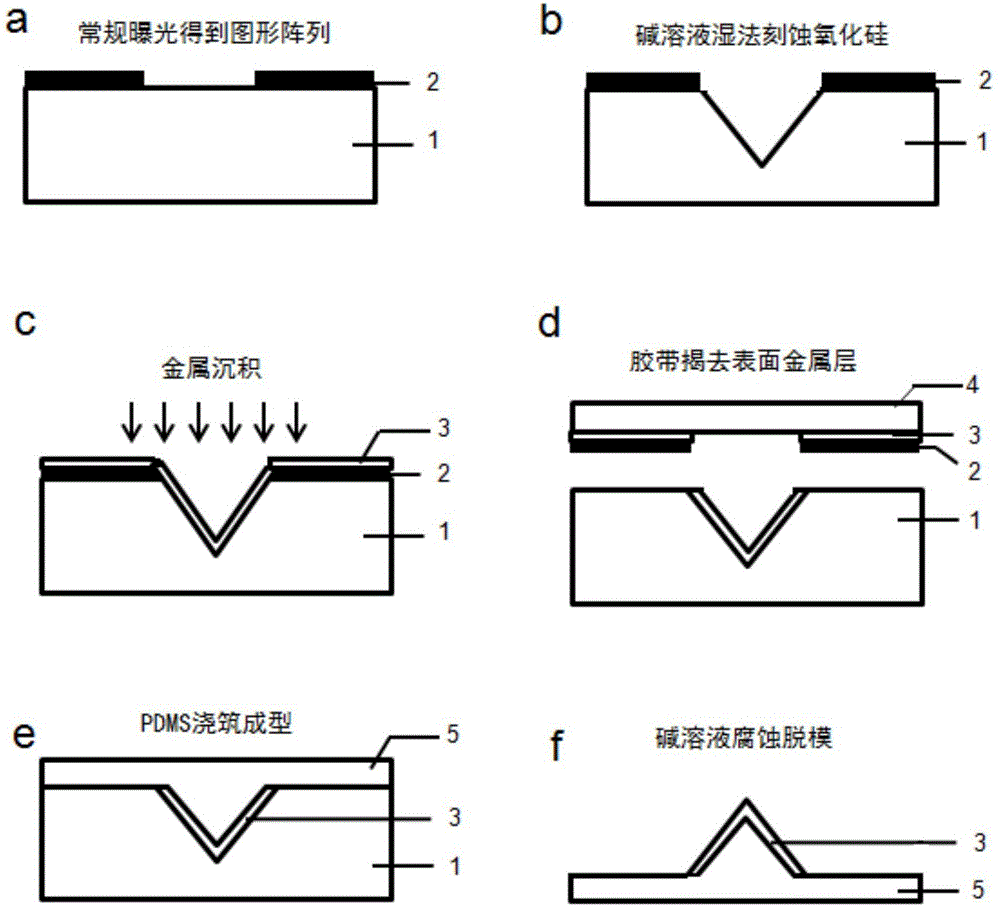
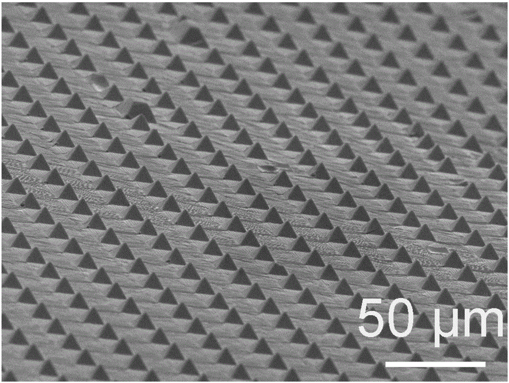
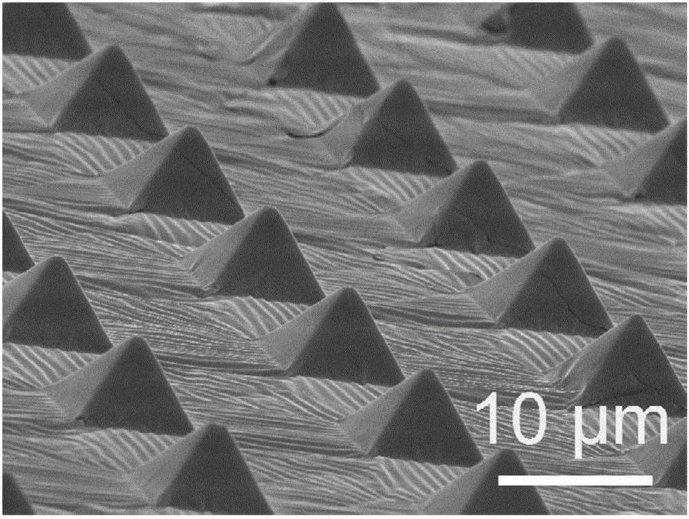
[0029] A method for preparing a large-area metal nano-tip array on a flexible substrate in this embodiment, such as figure 1 shown, including the following steps:

[0030] (1) On a clean silicon wafer substrate 1, a metallic chromium thin film is vapor-deposited, and the silicon wafer substrate 1 (the crystal direction of the silicon wafer is ) deposited with a 50 nanometer thick chromium thin film is cut into 1 cm × 1 cm. Sonicate the small piece with acetone, absolute ethanol, and deionized water for five minutes respectively, and dry it with high-purity nitrogen for later use; mark the above-mentioned single silicon wafer as sample i, and then spin-coat PMMA (polymethyl methacrylate) on sample i ) in chloroform solution (the weight-average molecular weight is 950K, and the mass percentage concentration of the photoresist is 6%), the spin coating speed is 4000rmp, and finally the glue is baked at 180°C for 4 minutes on a hot stage to obtain a photoresist with a thickness of ...

Embodiment 2

[0037] The technical solution of this embodiment is basically the same as that of Embodiment 1, except that the flexible soft mold material poured in step (6) is PVA (polyvinyl alcohol).

Embodiment 3

[0039] The technical solution of this embodiment is basically the same as that of Embodiment 1, except that the flexible soft mold material poured in step (6) is PMMA (polymethyl methacrylate).


PUM

PropertyMeasurementUnit
thicknessaaaaaaaaaa

Abstract

The invention discloses a preparing method for a large-area metal nanometer needle-tip array on a flexible substrate. The preparing method includes the following steps that (1) a metal chromium film is evaporated on the silicon slice substrate and coated with photoresist in a spinning mode; (2) a photoresist pattern with a hole array is prepared with the exposing-developing-fixing technology; (3) the portion, which is not protected by the photoresist pattern, of the metal chromium film is removed with ceric ammonium nitrate, and the surface of the silicon substrate at the bottom is exposed; (4) a silicon slice sample is etched with an alkali solution, and an inverted-pyramid silicon hole array is obtained; (5) a metal film is deposited on the surface of the sample, and a chromium metal layer and the deposited metal film on the surface of a silicon slice are removed in a stuck mode through adhesive tape; (6) the surface of the silicon slice is poured with a flexible soft mold material, the sample is corroded with an alkali solution, and finally the large-scale metal nanometer needle-tip array on the flexible substrate is obtained. The preparing method for the large-area metal nanometer needle-tip array on the flexible substrate has the advantages of being large in scale, low in cost and good in performance.

Description

technical field [0001] The invention relates to the field of nanotechnology, in particular to a method for preparing a large-area metal nano needle point array on a flexible substrate. Background technique [0002] Due to its special morphology, metal nanotips have important application prospects in micro-nano printing and plasmonic devices. First of all, the nano-tip is an important component of various current probe devices. The tiny structure of the tip can be used to realize the resolution and preparation of extremely small-sized nano-patterns. Expanded to the application field of micro-nano electrical characterization and detection; secondly, the nanostructure with the shape of the tip has a converging effect on the surface plasmon waves propagating on its surface, so in plasmonic catalysis and plasmonic heating etc. have important applications. [0003] The existing micro-nano processing technology has relatively mature process parameters for the preparation of nano-...

Claims


Application Information

Patent Timeline
Patent Type & Authority Applications(China)
IPC IPC(8): B82B3/00B82Y40/00
CPCB82B3/0014B82Y40/00
Inventor 孟秋实郭进曹国威周杰王俊
Owner CHINA ELECTRONIC TECH GRP CORP NO 38 RES INST
Why Eureka
Try Eureka