
Wafer fuse element having precut line substrate and manufacturing method thereof

A fuse and pre-cutting technology, applied in electrical components, semiconductor/solid-state device manufacturing, electric solid-state devices, etc., can solve the problems of manufacturers' troubles, hinder the smooth separation of substrate 8, and high cost control.

Active Publication Date: 2017-06-09
CHEERING SUN APPLIED MATERIALS
View PDF4 Cites 0 Cited by
  • Summary
  • Abstract
  • Description
  • Claims
  • Application Information

AI Technical Summary

Problems solved by technology

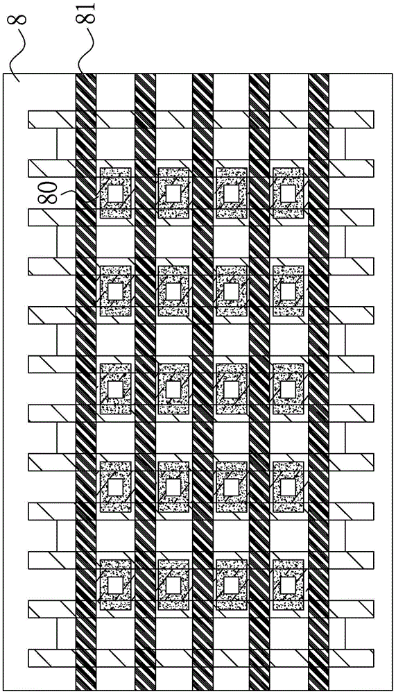
[0005] Since the substrate 8 and the silica gel layer 80 belong to the combination of different materials, the bonding strength of each other is not good, and the ductility between the two is very different. Even if the structure of the electrode part and the melt part can be protected, it will be covered. Staying at the position of the separation line 81 in the adjacent substrate, even if the separation line 81 is pre-formed with grooves or fractures to provide a structurally fragile part during separation, the existence of the silica gel layer 80 obviously hinders the smoothness of the separation of the substrate 8, Once an external force such as knocking or breaking is directly applied, the substrate 8 will be disconnected preferentially, while the silicone layer 80 may be disconnected later or even maintain a part of the connection, resulting in the destruction of the integrity of the preform itself.
Therefore, in the separation step of the above-mentioned existing technology, a laser or a diamond knife must be used to cut one by one along the separation line 81 to form multiple independent fuse elements. The production process is slow and the output efficiency cannot be improved, and the cost control is therefore high No less, undoubtedly causing troubles to manufacturers in this field

Method used


Image

  • Wafer fuse element having precut line substrate and manufacturing method thereof
  • Wafer fuse element having precut line substrate and manufacturing method thereof
  • Wafer fuse element having precut line substrate and manufacturing method thereof

Examples


Embodiment Construction

[0042] The aforementioned and other technical content, features and effects of the present invention will be clearly presented in the following detailed description of the preferred embodiments in conjunction with the accompanying drawings; in addition, in each embodiment, the same elements will be similar The label indicates.

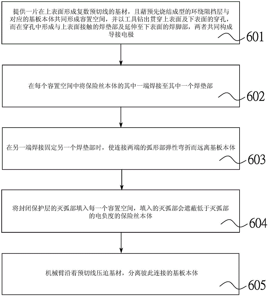
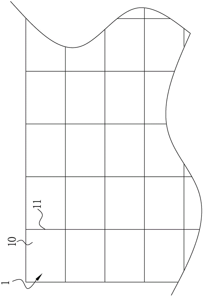
[0043] The manufacturing process of the first preferred embodiment of the present invention is as follows figure 2 As shown in the flow chart of , first, as in step 601 and image 3As shown, a piece of base material made of ceramic material is pre-divided into a plurality of substrate bodies 1 connected to each other, and there are pre-cut lines 11 formed on the upper surface 10 such as concave grooves between the substrate bodies 1 adjacent to each other, so as to facilitate the production process. After the end, it is easy to apply external force to quickly separate the entire row of preforms from the adjacent row, and then separate the entire row ...


PUM


Abstract

The invention provides a wafer fuse element having a precut line substrate for surface mounting to a circuit board. The wafer fuse element comprises a substrate body having an upper surface, a lower surface and two end rims connected the upper surface with the lower surface, the substrate body is provided with precut lines corresponding to the two end rims on one of the upper surface and the lower surface; a pair of separate conductive electrodes, the conductive electrodes comprise welding pad portions arranged on the supper surface and welding pin portions extending from the welding pad portions to the lower surface; a surrounding blocking layer which is arranged on the supper surface and is used for sealing and surrounding the welding pad portions, the surrounding blocking layer and the substrate body commonly form an accommodation space, the precut lines are not covered by the surrounding blocking layer and are exposed outside; a fuse body which is arranged in the accommodation space, two ends of the fuse body are respectively welded with the welding pad portions; and a sealing protection layer used for sealing and blocking the accommodation space.

Description

technical field [0001] The invention relates to a chip fuse element with a pre-cut substrate and its manufacturing method, in particular to a chip fuse element which is easy to cut and separate and its manufacturing method. Background technique [0002] A fuse is a disposable component connected to a circuit to protect the circuit, usually made of low-resistance metal or alloy system wire or sheet material, such as lead-tin alloy, aluminum, copper, silver, Copper-manganese alloy and copper-silver alloy, etc., IEC127 standard defines it as a fuse (fuse-link), a general fuse is composed of three parts, one of which is the fuse part as the core of the fuse, which plays the role of cutting off the current when it is blown The second is that the electrode part is used to connect the melt and the circuit, and must have good conductivity; the last bracket part is to make the aforementioned parts together form a rigid structure, which improves the convenience of installing or using ...

Claims


Application Information

Patent Timeline
IPC IPC(8): H01L23/525H01L21/768
CPCH01L23/5256H01L21/76838H01L2221/1068
Inventor 庄弘毅凌溢骏曾国书
Owner CHEERING SUN APPLIED MATERIALS
Learn More