Fly-back type switching power supply
A switching power supply, flyback technology, applied in the direction of electrical components, adjusting electrical variables, high-efficiency power electronic conversion, etc., can solve the problems of high cost, poor loop response, complex process, etc., to achieve good bandwidth, good EMI performance, The effect of high conversion efficiency
- Summary
- Abstract
- Description
- Claims
- Application Information
AI Technical Summary
Problems solved by technology
Method used
Image
Examples
no. 1 example
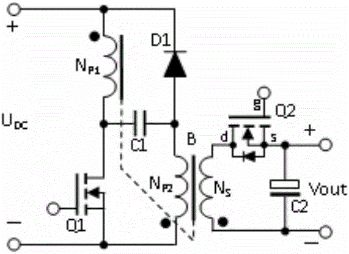
[0036] figure 2 The schematic diagram of the flyback switching power supply according to the first embodiment of the present invention is shown, including a transformer B, a first switching tube Q1 and a second switching tube Q2, both of which are N-channel field effect transistors, a second capacitor C2, and a second switching tube Q2. A diode D1, the transformer B includes the first primary winding N P1 , the second primary winding N P2 and the secondary winding N S , secondary winding N S The opposite end is connected to the drain d of the second switching tube Q2, the source s of the second switching tube Q2 is connected to one end of the second capacitor C2, and forms a positive output, which is the + end of Vout in the figure, and the same end of the secondary winding NS is connected to The other end of the second capacitor C2 is connected to form a negative output, which is the - end of Vout in the figure; input DC power U DC The positive terminal + simultaneously ...
no. 2 example
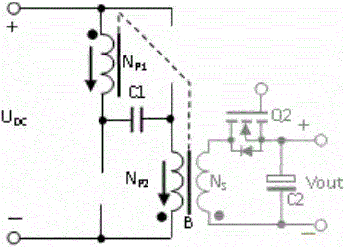
[0074] The present invention also provides an equivalent solution to the above-mentioned first embodiment, corresponding to solution 2, see image 3 , a flyback switching power supply, including a transformer B, the first switch tube Q1, the second switch tube Q2, both of which are N-channel field effect transistors, the second capacitor C2, the first diode D1, and the transformer B includes the first One primary winding N P1 , the second primary winding N P2 and the secondary winding N S , secondary winding N S The opposite terminal is connected to the drain d of the second switching tube Q2, the source s of the second switching tube Q2 is connected to one end of the second capacitor C2, and forms a positive output, which is the + terminal of Vout in the figure, and the secondary winding N S The end with the same name is connected to the other end of the second capacitor C2 to form a negative output, which is the - end of Vout in the figure; the input DC power supply U DC...
no. 3 example
[0091] see Figure 4 , which is also the aforementioned solution three, a flyback switching power supply, including a transformer B, a first switching tube Q1, a second switching tube Q2, the first switching tube Q1 is a P-channel field effect tube, and the second switching tube Q2 is An N-channel field effect transistor, a second capacitor C2, a first diode D1, and a transformer B including a first primary winding N P1 , the second primary winding N P2 and the secondary winding N S , secondary winding N S The opposite terminal is connected to the drain d of the second switching tube Q2, the source s of the second switching tube Q2 is connected to one end of the second capacitor C2, and forms a positive output, which is the + terminal of Vout in the figure, and the secondary winding N S The end with the same name is connected to the other end of the second capacitor C2 to form a negative output, which is the - end of Vout in the figure; the input DC power supply U DC The n...
PUM
 Abstract
Description
Claims
Application Information


