A silicon-based te-mode polarizer based on an asymmetric directional coupler

A directional coupler, asymmetric technology, applied in the field of integrated optics, can solve the problems of high insertion loss and large transmission loss of the mode analyzer, and achieve the effects of reduced insertion loss, low insertion loss and large operating bandwidth

Active Publication Date: 2019-04-30
SOUTHEAST UNIV
View PDF4 Cites 0 Cited by
  • Summary
  • Abstract
  • Description
  • Claims
  • Application Information

AI Technical Summary

Problems solved by technology

At present, the mode analyzer based on the hybrid plasmonic waveguide structure has gradually become a research hotspot, because the device based on this structure is compatible with the SOI material system and exhibits relatively good performance, but due to the introduction of metal materials, the ohmic loss of the hybrid plasmonic waveguide Compared with the transmission loss of the dielectric waveguide, the insertion loss of the mode analyzer based on a single hybrid plasmonic waveguide structure is generally high

Method used


Image

  • A silicon-based te-mode polarizer based on an asymmetric directional coupler
  • A silicon-based te-mode polarizer based on an asymmetric directional coupler
  • A silicon-based te-mode polarizer based on an asymmetric directional coupler

Examples


Embodiment 1

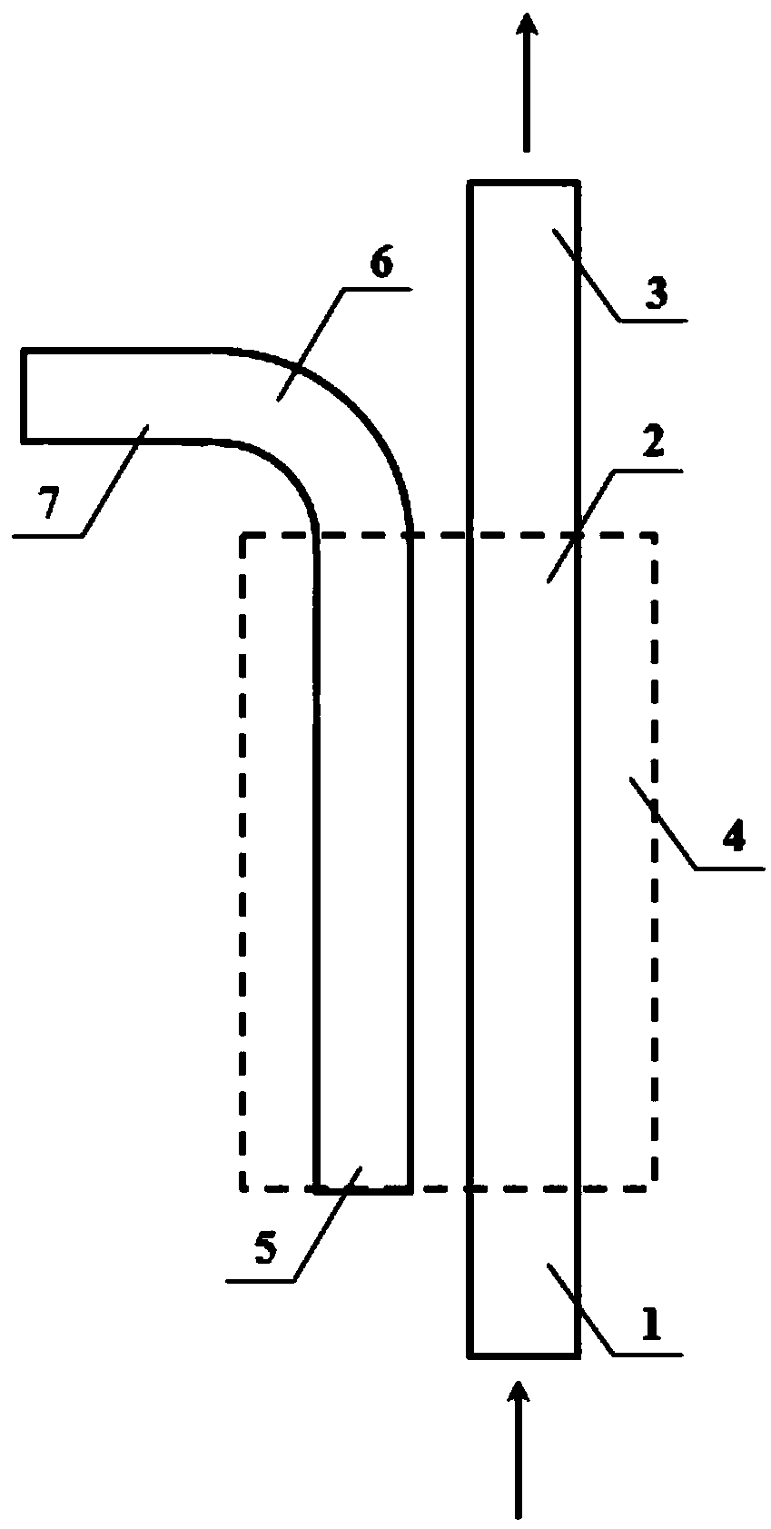
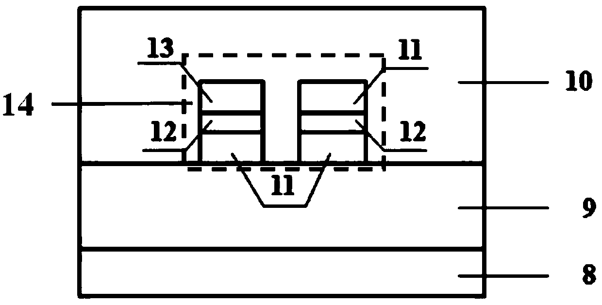
[0038] Such as figure 1 and figure 2 As shown, the analyzer consists of a silicon-based substrate 8, a buried oxide layer 9, an analyzer component 14, and an upper cladding layer 10 from bottom to top, wherein the buried oxide layer 9 is grown on the upper surface of the silicon-based substrate 8, the upper The cladding layer 10 covers the upper surface of the buried oxide layer 9, and the analyzer component 14 grows horizontally on the upper surface of the buried oxide layer 9 and is covered by the upper cladding layer 10;

[0039] The polarization analysis unit 14 includes an input channel 1, a right straight channel 2, an output channel 3, a left straight channel 5, a left curved channel 6 and a left horizontal channel 7;

[0040] One end of the right direct channel 2 is connected to the input channel 1, and the other end is connected to the output channel 3;

[0041] One end of the left curved channel 6 is connected to the left straight channel 5, and the other end is c...

Embodiment 2

[0055] Such as Figure 8 As shown in the schematic diagram of the improved polarization analyzer 14 (silicon-based substrate 8, buried oxide layer 9 and upper cladding layer 10 are exactly the same as those in Embodiment 1), the improved polarization analyzer 14 includes an input channel 1 and a right through channel 2 , output channel 3, left straight channel 5, left curved channel 6 and left horizontal channel 7;

[0056] One end of the right direct channel 2 is connected to the input channel 1, and the other end is connected to the output channel 3;

[0057] One end of the left curved channel 6 is connected to the left straight channel 5, and the other end is connected to the left horizontal channel 7; wherein, the output channel 3 and the left curved channel 6 are located at the same end;

[0058] The input channel 1, the right straight channel 2 and the output channel 3 are all silicon-based horizontal groove waveguides, and the left straight channel 5, left curved chann...


PUM


Abstract

The invention discloses a silicon-based TE mode analyzer based on an asymmetric directional coupler. The analyzer orderly comprises a silicon-based substrate (8), a buried oxide layer (9), an analyzer component (14) and an upper cladding layer (10) from the bottom to top, wherein the buried oxide layer (9) is grown at the upper surface of the silicon-based substrate (8), the upper cladding layer (10) covers the upper surface of the buried oxide layer (9), the analyzer component (14) is grown at the upper surface of the buried oxide layer (9) and is covered by the upper cladding layer (10), and the analyzer component (14) comprises an input channel (1), a right through channel (2), an output channel (3), a left through channel (5), a left curved channel (6), and a left horizontal channel (7). According to the silicon-based TE mode analyzer, the insertion loss of the analyzer is effectively reduced, the extinction ratio of a device is raised, and the size of the device is reduced.

Description

technical field [0001] The invention relates to a silicon-based TE mode polarizer based on an asymmetric directional coupler, belonging to the technical field of integrated optics. Background technique [0002] In recent years, silicon-on-insulator (SOI) materials have attracted widespread attention due to their compatibility with mature complementary metal-oxide-semiconductor (CMOS) processes and their ability to effectively reduce device sizes. However, the birefringence caused by the large refractive index difference between the cladding layer and the core layer in SOI materials greatly restricts the wider and deeper application of this material system in integrated photonics. In order to alleviate the negative impact of birefringence , a variety of polarization processing devices were designed and manufactured. Among them, the analyzer is widely used in the photon circuit because it can eliminate the unnecessary polarized light in the optical path; generally, the mode a...

Claims


Application Information

Patent Timeline
Patent Type & Authority Patents(China)
IPC IPC(8): G02B6/126
CPCG02B6/126
Inventor 肖金标倪斌
Owner SOUTHEAST UNIV
Why Eureka
Try Eureka