Graphic photomask connecting hole defect inspection test structure and method

A technology for testing structure and defect inspection, which is applied in the field of semiconductor technology, and can solve the problems of recognition, difficult detection of pattern mask defects, detection rate, and inability to calculate pattern mask defects, so as to achieve accurate inspection results and eliminate groove interference , The effect of saving process procedures

Active Publication Date: 2017-06-30
SHANGHAI HUALI MICROELECTRONICS CORP
View PDF5 Cites 5 Cited by
  • Summary
  • Abstract
  • Description
  • Claims
  • Application Information

AI Technical Summary

Problems solved by technology

[0003] First, through OPC (Optical Proximity Correction, optical proximity correction) calculation to find out the defects of the mask, but due to the increase in the complexity of the graphic mask, OPC cannot calculate the shortcomings of all types of graphic masks;
[0004] Second, detect the defect of the connection hole 01 on the wafer through the lithography energy / focal length matrix, and then confirm the defect of the mask through SEM observation. This method can effectively detect the defect of the graphic mask in other graphic layers, but for The hole-like structure in the hole pattern layer, such as contact hole and connection hole 01, etc., this method has great disadvantages. The structure formed after tape-out according to the conventional process of 28nm products is as follows: figure 1 As shown, the connection holes 01 need to be connected by trenches, because within the range of the process window, due to the interference of the trench formation process, it is often difficult to detect the deformation of the connection holes 01 and similar pattern mask defects or the detection rate Very low, or difficult to identify with engineering judgment

Method used


Image

  • Graphic photomask connecting hole defect inspection test structure and method
  • Graphic photomask connecting hole defect inspection test structure and method
  • Graphic photomask connecting hole defect inspection test structure and method

Examples


Embodiment Construction

[0024] In order to make the above objects, features and advantages of the present invention more comprehensible, specific implementations of the present invention will be described in detail below in conjunction with the accompanying drawings.

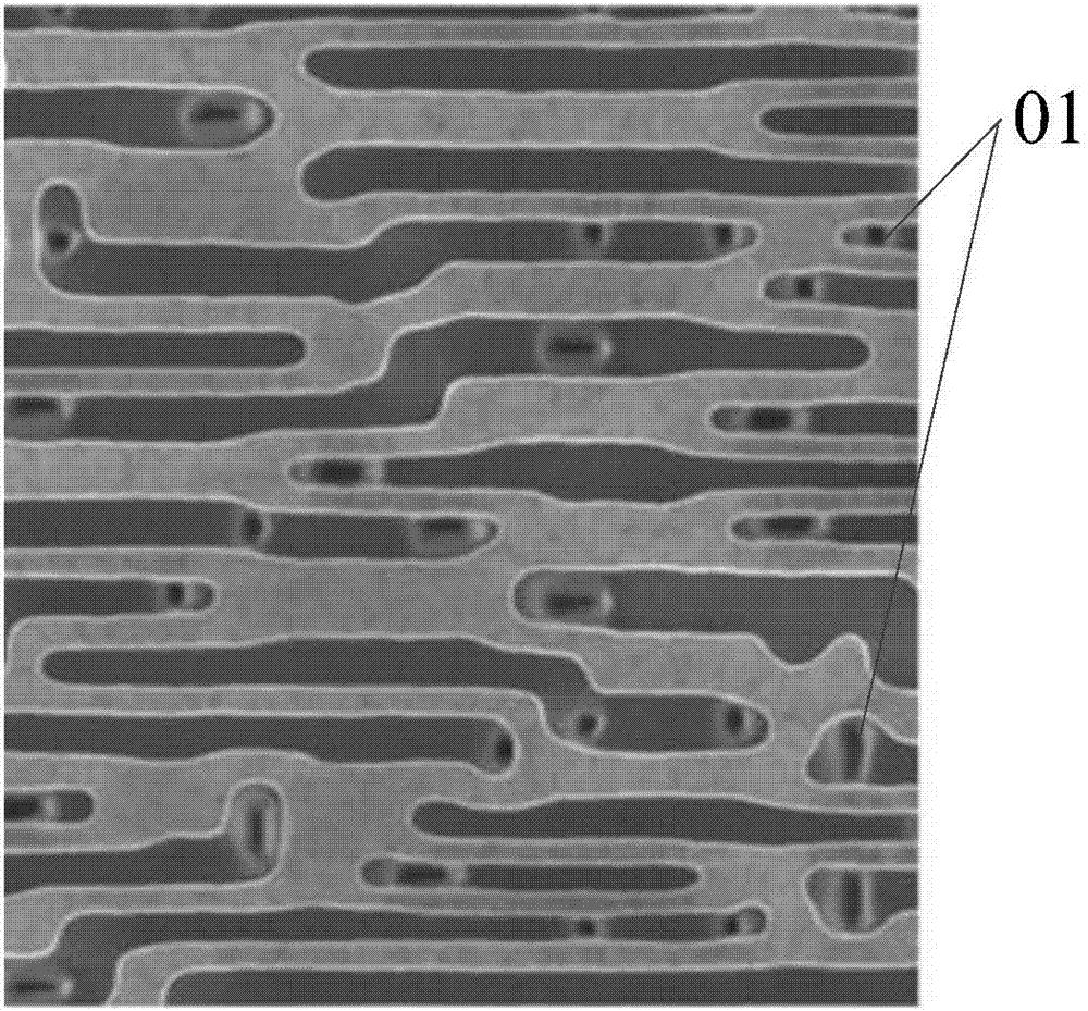
[0025] Please refer to Figure 6 , in order to be able to conveniently check the defects of the connection holes on the existing pattern mask, the present invention provides a test structure using the existing pattern mask as the connection hole photolithography mask, and its manufacturing method comprises the following steps:

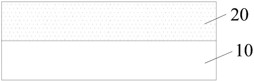
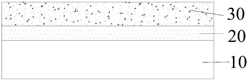
[0026] Step 1: Please refer to figure 2 and image 3 , providing a substrate 10 for well ion and source-drain ion implantation, the combination type of these two processes can be selected from N-WELL / PMOS, N-WELL / NMOS, P-WELL / PMOS, P-WELL / NMOS, etc., That is to say, the well ion implantation layer 20 can be an N well area or a P well area, and the source-drain ion implantation 30 can be N-type doped or P-typ...


PUM


Abstract

The invention provides a graphic photomask connecting hole defect inspection test structure and method. Trap ion and source and drain ion injection is performed on a substrate and then a metal silicide layer is deposited, and holes or grooves are formed through photoetching; a metal silicide barrier layer is deposited in the holes or the grooves, a metal layer is deposited on the metal silicide layer and a first dielectric layer is deposited on the metal silicide barrier layer; then a second dielectric layer is deposited on the structure and connecting holes are formed on the second dielectric layer, the connecting holes on the test structure are formed by the tested graphic photomask through photoetching, and then metal deposition is performed on the connecting holes so as to form metal plugs; and electron beam scanning is performed, i.e. the brightness of each connecting hole under an electron microscope is scanned to determine the defect of the connecting holes so that the defect of the connecting hole patterns on the graphic photomask can be found. According to the test structure, the problem that the connecting holes are interfered by the grooves can be eliminated so that the defect only caused by the connecting hole patterns of the graphic photomask can be purely found.

Description

technical field [0001] The invention relates to the field of semiconductor technology, in particular to a defect inspection and testing structure and method for connection holes of a graphic mask. Background technique [0002] With the development of integrated circuit technology and the scaling down of critical dimensions, the semiconductor technology is becoming more and more complex. In the process of product development with a minimum line width of 28nm, point defects on the graphic mask are the biggest barriers to the conduction of the upper and lower lines of the product. hinder. There are generally two methods for traditionally detecting pattern mask defects: [0003] First, through OPC (Optical Proximity Correction, optical proximity correction) calculation to find out the defects of the mask, but due to the increase in the complexity of the graphic mask, OPC cannot calculate the shortcomings of all types of graphic masks; [0004] Second, detect the defect of the ...

Claims


Application Information

Patent Timeline
Patent Type & Authority Applications(China)
IPC IPC(8): H01L21/66
Inventor 范荣伟陈宏璘龙吟倪棋梁
Owner SHANGHAI HUALI MICROELECTRONICS CORP
Why Eureka
Try Eureka