Semiconductor element and method for manufacturing the same

A manufacturing method and semiconductor technology, applied in semiconductor devices, electrical components, electrical solid-state devices, etc., can solve the problems of reducing image resolution and increasing noise, and achieve the effects of improving image resolution, reducing optical path difference, and reducing noise.

Active Publication Date: 2017-06-30
POWERCHIP SEMICON MFG CORP
View PDF4 Cites 1 Cited by
  • Summary
  • Abstract
  • Description
  • Claims
  • Application Information

AI Technical Summary

Problems solved by technology

However, when the light passes through the light pipe structure, it is easy to cause the light scattering (light scattering) to the area outside the light pipe structure because the incident angle is too large
This situation will cause cross-talk phenomenon, which will increase the noise received by the CMOS image sensor, thereby reducing the image resolution.

Method used


Image

  • Semiconductor element and method for manufacturing the same
  • Semiconductor element and method for manufacturing the same
  • Semiconductor element and method for manufacturing the same

Examples


Embodiment Construction

[0053] The present invention will be described more fully with reference to the accompanying drawings of this embodiment. However, the present invention can also be embodied in various forms and should not be limited to the embodiments described herein. In the drawings, the thicknesses of layers and regions may be exaggerated for clarity. The same or similar reference numerals denote the same or similar elements, and the following paragraphs will not repeat them one by one.

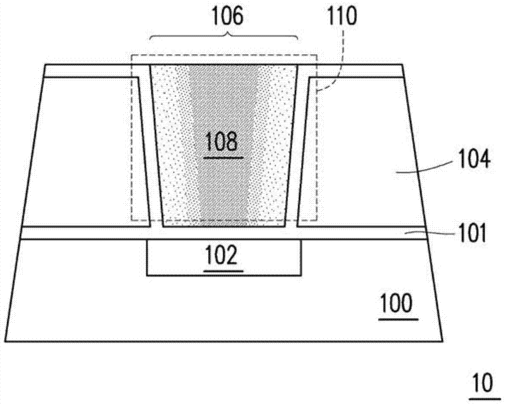
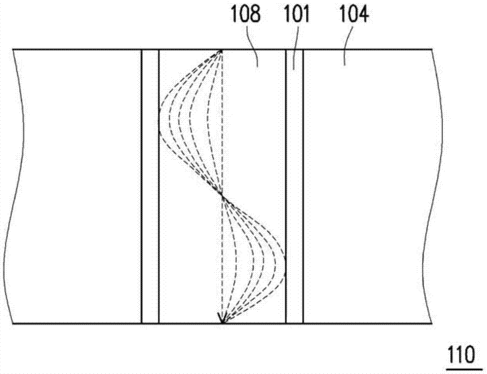
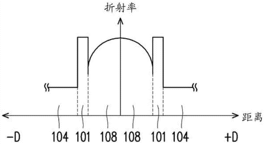
[0054] figure 1 is a schematic cross-sectional view of a semiconductor device according to the first embodiment of the present invention. Figure 2A yes figure 1 Partially enlarged cross-sectional schematic diagram. Figure 2B yes Figure 2A The refractive index distribution diagram.

[0055] Please refer to figure 1 , the semiconductor device 10 according to the first embodiment of the present invention includes a substrate 100 , a sensor 102 , a dielectric layer 104 and a light pipe structure 108...


PUM


Abstract

The present invention discloses a semiconductor element and a method for manufacturing the same. The semiconductor element includes a substrate, a sensor, a dielectric layer, and a light pipe structure. The sensor is located in the substrate. The dielectric layer is located on the substrate. The light pipe structure is filled into the grooves in the dielectric layer. The light pipe structure corresponds to the sensor. The light pipe structure has a graded refractive index. The graded refractive index decreases from the center of the light pipe structure to the peripheral area.

Description

technical field [0001] The present invention relates to an integrated circuit and its manufacturing method, and in particular to a semiconductor element with a light guide structure of graded refractive index and its manufacturing method. Background technique [0002] An image sensor is a device that converts an optical image into an electronic signal, and it is widely used in digital cameras and other electronic optical devices. Early image sensors used analog signals, such as video camera tubes. Currently, image sensors are mainly classified into charge-coupled device (CCD) type and complementary metal oxide semiconductor (CMOS) type. [0003] A CMOS image sensor is a component that uses CMOS manufacturing technology to convert optical images into electrical signals. Compared with the CCD type image sensor, the CMOS sensor can make the signal processing circuit into a single chip, which can not only reduce the size of the product, but also be compatible with CMOS technol...

Claims


Application Information

Patent Timeline
Patent Type & Authority Applications(China)
IPC IPC(8): H01L27/146
CPCH01L27/146H01L27/14625H01L27/14643H01L27/14683
Inventor 李世平陈昱安黄绣雯张娟华
Owner POWERCHIP SEMICON MFG CORP
Why Eureka
Try Eureka