A kind of semiconductor device and its preparation method, electronic device

An electronic device and semiconductor technology, which is applied in the manufacture of semiconductor/solid-state devices, circuits, transistors, etc., can solve the problems of semiconductor device threshold voltage degradation and missing top of the gate structure, achieve stable threshold voltage, consistent etching rate, and improve performance and yield effect

Active Publication Date: 2020-04-10
SEMICON MFG INT (SHANGHAI) CORP +1
View PDF6 Cites 0 Cited by
  • Summary
  • Abstract
  • Description
  • Claims
  • Application Information

AI Technical Summary

Problems solved by technology

However, defects in the outline of the NMOS gate structure usually occur in the device prepared by the method, for example, a defect appears on the top of the gate structure, forming a gap
[0004] By analyzing the defect, it is found that the cause of the structure is due to the implantation of P ions to the NMOS before etching. The current solution is usually to perform rapid thermal annealing after the NMOS pre-doped ion implantation to The phosphorus doped in the NMOS is diffused to the inside, but the method will cause the B doped in the PMOS to quickly diffuse to the NMOS, so some regions may be shared between the NMOS and the PMOS, thereby causing the threshold voltage of the semiconductor device to occur. degradation

Method used


Image

  • A kind of semiconductor device and its preparation method, electronic device
  • A kind of semiconductor device and its preparation method, electronic device
  • A kind of semiconductor device and its preparation method, electronic device

Examples


Embodiment 1

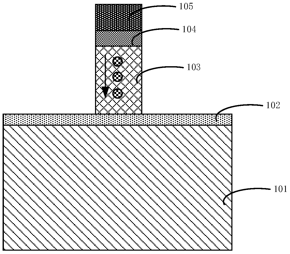
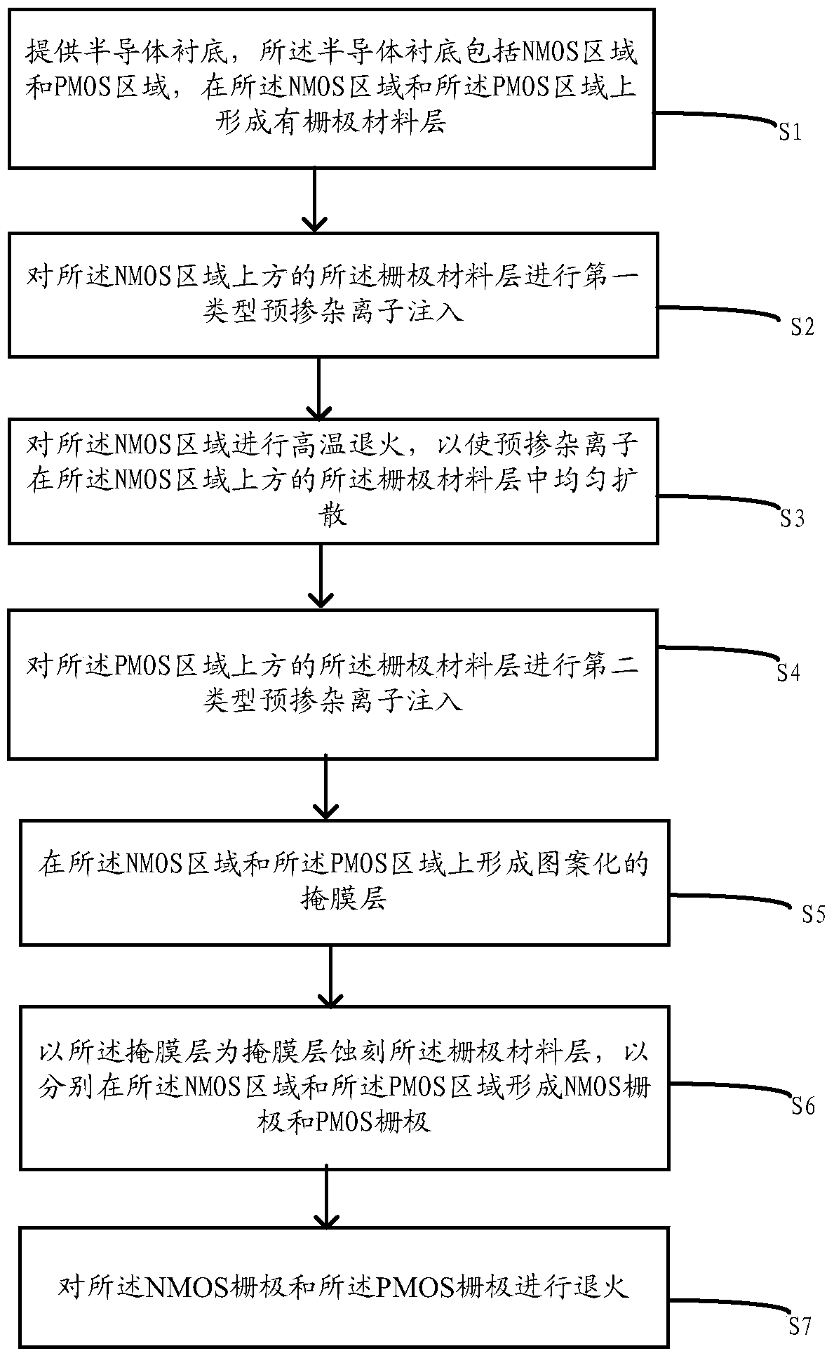
[0038] In order to solve the problems in the prior art, the present invention provides a method for preparing a semiconductor device, the following in conjunction with the attached figure 1 A specific embodiment of the present invention will be further described.

[0039] Step 101 is executed to provide a semiconductor substrate 101 , the semiconductor substrate includes an NMOS region and a PMOS region, and a gate material layer 103 is formed on the NMOS region and the PMOS region.

[0040] First, refer to figure 1 , a semiconductor substrate 101 is provided, and the semiconductor substrate 101 may be at least one of the materials mentioned below: silicon, silicon-on-insulator (SOI), silicon-on-insulator (SSOI), and the like.

[0041] In addition, an active region may be defined on the semiconductor substrate 101 . Other active devices may also be included on the active area, which are not marked in the shown figures for convenience.

[0042]Then shallow trench isolation i...

Embodiment 2

[0083] The present invention also provides a semiconductor device, which is prepared by the method described in the first embodiment. The semiconductor device prepared by the method solves the problem of missing and gaps caused by over-etching the top of the NMOS gate in the prior art, and can also prevent the pre-doped ions in the PMOS from diffusing to the NMOS region, making the threshold voltage more stable and further improving performance and yield of semiconductor devices.

Embodiment 3

[0085] The present invention also provides an electronic device, including the semiconductor device described in the second embodiment. Wherein, the semiconductor device is the semiconductor device described in the second embodiment, or the semiconductor device obtained according to the preparation method described in the first embodiment.

[0086] The electronic device of this embodiment can be any electronic product or equipment such as mobile phone, tablet computer, notebook computer, netbook, game console, TV set, VCD, DVD, navigator, camera, video recorder, voice recorder, MP3, MP4, PSP, etc. , can also be any intermediate product including the semiconductor device. The electronic device according to the embodiment of the present invention has better performance due to the use of the above-mentioned semiconductor device.


PUM

PropertyMeasurementUnit
thicknessaaaaaaaaaa

Abstract

The invention relates to a semiconductor device and a preparation method thereof, and an electronic apparatus. The method comprises the following steps: providing a semiconductor substrate, wherein the semiconductor substrate includes an NMOS region and a PMOS region, and a gate material layer is formed on the NMOS region and the PMOS region; performing first-type pre-doped ion implantation on the gate material layer above the NMOS region; performing high-temperature annealing on the NMOS region to evenly disperse pre-doped ions in the gate material layer above the NMOS region; and performing second-type pre-doped ion implantation different from the first-type pre-doped ion implantation on the gate material layer above the PMOS region. Pre-doped ions in the PMOS region can be prevented from diffusing into the NMOS region. The threshold voltage is more stable. The performance and yield of the semiconductor device are improved.

Description

technical field [0001] The present invention relates to the field of semiconductors, in particular, the present invention relates to a semiconductor device, a preparation method thereof, and an electronic device. Background technique [0002] With the continuous development of integrated circuit technology, more devices will be integrated on the chip, and the chip will also have faster speed. Driven by these requirements, the geometric size of devices will continue to shrink, and new materials, new technologies and new manufacturing processes will be continuously used in the chip manufacturing process. At present, the manufacturing process of semiconductor devices is gradually mature. [0003] With the continuous reduction of the size of semiconductor devices, more challenges are brought to the device preparation. At present, the preparation method of transistors in semiconductor devices is usually to form NMOS and PMOS gate material layers first, and then perform pre-doped...

Claims


Application Information

Patent Timeline
Patent Type & Authority Patents(China)
IPC IPC(8): H01L21/8238H01L27/092
CPCH01L21/823828H01L27/092
Inventor 何丽丽徐宽陈荣堂
Owner SEMICON MFG INT (SHANGHAI) CORP
Why Eureka
Try Eureka