A method for growing polysilicon target material

A technology for growing polycrystalline and silicon targets, applied in the directions of crystal growth, single crystal growth, single crystal growth, etc., can solve the problems of large differences, lack of control means for crystal production rate, large product size, etc., to improve crystal grains Size and uniformity, the effect is timely and obvious, and the effect of overcoming the large grain size

Inactive Publication Date: 2019-06-25
HEBEI UNIV OF TECH
View PDF4 Cites 0 Cited by
  • Summary
  • Abstract
  • Description
  • Claims
  • Application Information

AI Technical Summary

Problems solved by technology

[0006] Second, the crystal grains are large and uneven
The first is that the solid-liquid interface protrudes too much during the solidification process (it can be approximately reflected from the shape of the top of the finished crystal), the environment of each part (such as temperature, pressure, etc.) is quite different, and the product size is too large, which affects each part of the crystal. The production rate lacks control means, and the effect of process control is not timely or obvious

Method used


Image

  • A method for growing polysilicon target material
  • A method for growing polysilicon target material
  • A method for growing polysilicon target material

Examples


Embodiment 1

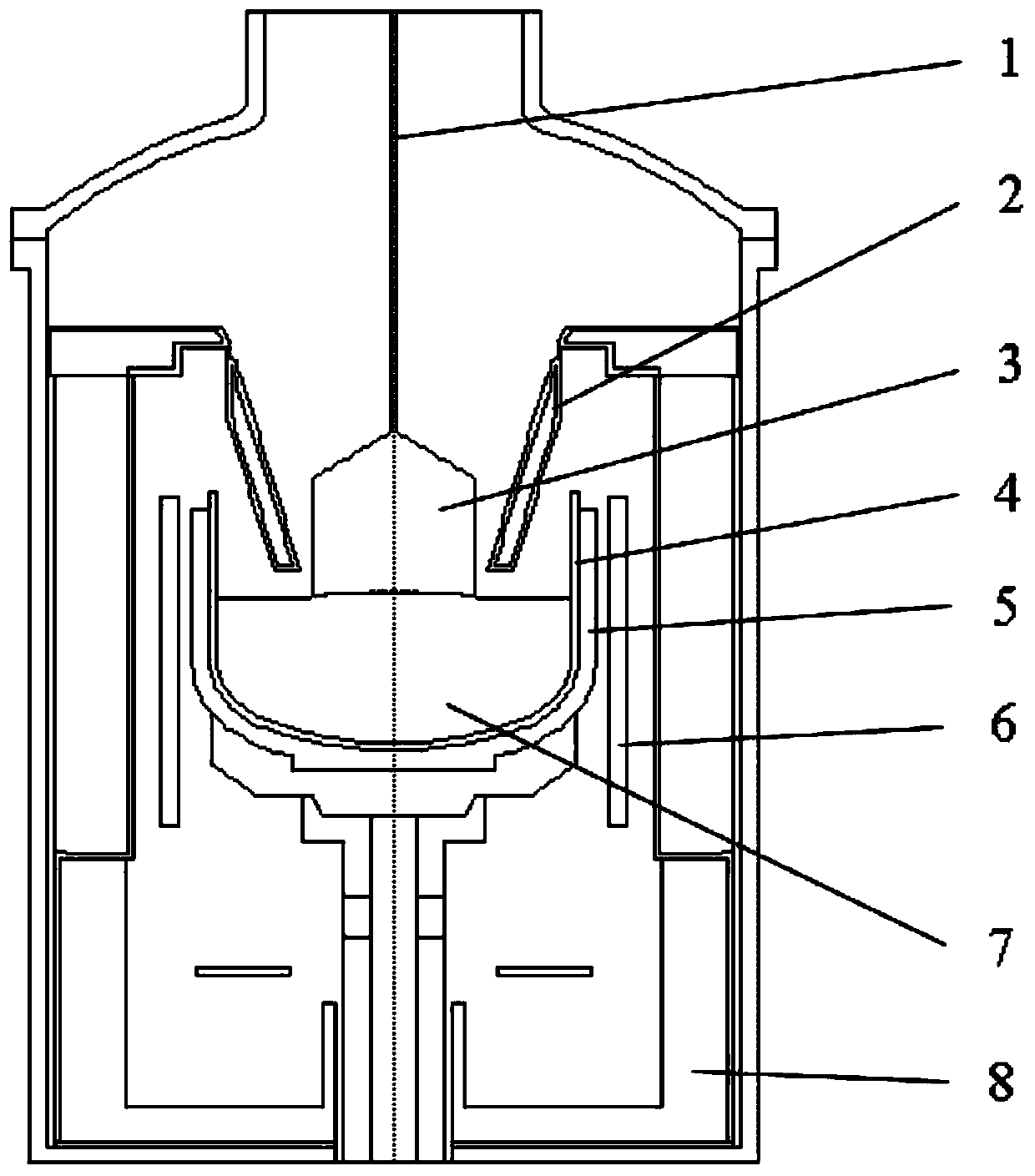
[0052] The crystal pulling furnace used in the method for growing a polysilicon target in this embodiment is a crystal pulling furnace of the model JRDL-900; the crystal pulling furnace includes a pulling device and a growth furnace part, and the pulling device includes a crystal lifting and rotating mechanism 1, The crystal ascending and rotating mechanism 1 is connected to the seed chuck through the seed rod, and the crystal ascending and rotating mechanism is used to pull the polysilicon 3; the cavity of the growth furnace part is provided with a guide tube 2, a quartz crucible 4, a graphite crucible 5 and a heater 6 , the quartz crucible 4 is placed in the graphite crucible 5, heated by the heater 6, the polysilicon raw material is placed in the quartz crucible, and the molten silicon 7 is obtained after heating; an insulating material 8 is arranged outside the furnace cavity for heat preservation; The cylinder is used to improve the temperature field and flow field in the ...

Embodiment 2

[0079] The specific steps of the method in this embodiment are the same as in Example 1, and the required diameter of the designed product and the crystal orientation of the used seed crystal are also the same for , the difference is that:

[0080] The second step, chemicals:

[0081] Fill the crystal pulling furnace with argon gas at a flow rate of 100L / h until the furnace pressure is 3000Pa, then set the heating power to 180kw, and change the polysilicon raw material in the crystal pulling furnace. , to obtain molten silicon 7;

[0082] The third step, seeding:

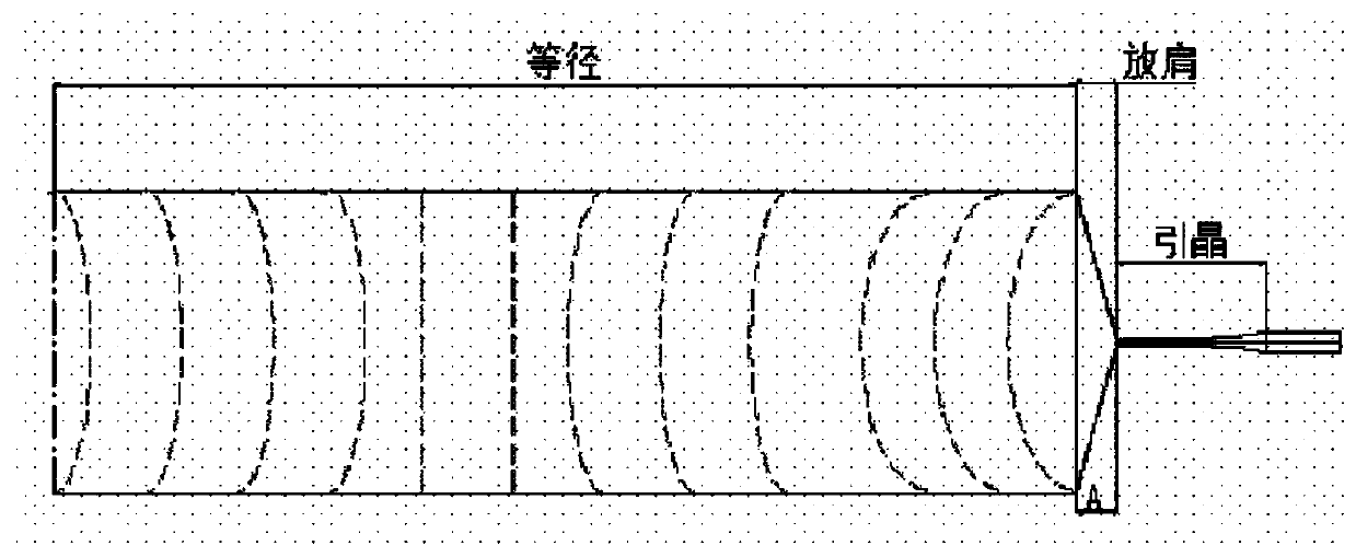
[0083] After the polysilicon raw materials are prepared, the heating power electric control controller is adjusted to automatic, the heating power is reduced to the size required for seeding, the temperature is lowered to make the liquid level of the molten silicon 7 supercooled, and the seeding on the pulling device is reduced. crystal rod, so that the bottom surface of the seed crystal contacts the molten silico...


PUM

PropertyMeasurementUnit
widthaaaaaaaaaa
thicknessaaaaaaaaaa
diameteraaaaaaaaaa

Abstract

The invention relates to a method for growing a polycrystalline silicon target material. The method comprises the following processes of charging a furnace, melting a material, seeding, shouldering, rotating shoulder, obtaining equal diameter and ending, wherein the seeding process comprises the following steps: after a polycrystalline silicon raw material is melt, reducing heating power to the size required by seeding, and reducing the temperature until the liquid level of molten silicon has supercooling degree; reducing a seed crystal rod on a lifting device, and enabling the bottom surface of a seed crystal to make contact with the molten silicon; when a diaphragm at a contact position between the seed crystal and the molten silicon is detected to be stable, upward lifting the seed crystal at the crystal lifting speed of 3 to 7mm / min, and solidifying a crystal when a contact surface between the seed crystal and the molten silicon grows along with the lifting of the seed crystal; when the size of the obtained crystal is kept at 3 to 5mm, and the length is 160 to 190mm, obtaining a fine crystal, further reducing the crystal lifting speed and turning into a shouldering stage; the shouldering process comprises the following steps: reducing the crystal lifting speed to be 0.4 to 0.8mm / min; meanwhile, carrying out linear temperature reduction at the temperature reduction speed of 15 to 25DEG C / hr, shouldering the crystal, and stopping linear temperature reduction until the diameter of the crystal is smaller than the diameter of 5 to 7mm required by the product.

Description

technical field [0001] The invention relates to the technical field of polysilicon targets, in particular to a method for growing polysilicon targets. Background technique [0002] The target is the basic consumable in the process of preparing functional thin films by magnetron sputtering. The quality of the target material plays a crucial role in the performance of the thin film. Silicon target is a simple sputtering target source, which is mainly used for magnetron sputtering to prepare thin films such as silicon and silicon dioxide. It has important applications in information storage, low-e glass, LCD flat panel display, solar cells and other fields. [0003] Silicon target products are divided into single crystal silicon target and polycrystalline silicon target. Compared with single crystal silicon target, polycrystalline silicon target is easy to stimulate, has lower cost and large output. Further improving the quality of polysilicon targets is the main goal at this...

Claims


Application Information

Patent Timeline
Patent Type & Authority Patents(China)
IPC IPC(8): C30B28/10C30B29/06C23C14/35
CPCC23C14/3414C23C14/35C30B28/10C30B29/06
Inventor 陈洪建王佳阎文博张恩怀
Owner HEBEI UNIV OF TECH
Why Eureka
Try Eureka