

Method of manufacturing semiconductor device, array substrate and display apparatus
An array substrate and semiconductor technology, applied in semiconductor devices, semiconductor/solid-state device manufacturing, electrical solid-state devices, etc., can solve problems such as not achieving significant results, and achieve the effects of improving electrical performance, reducing contact resistance, and low defects
- Summary
- Abstract
- Description
- Claims
- Application Information
AI Technical Summary
Problems solved by technology
Method used
Image


Examples
example 1
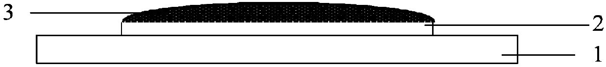
[0049] First, a gate and a gate insulating layer are formed on a glass substrate. Then, a first oxide semiconductor layer having a thickness of 20 nm was formed by deposition on the gate insulating layer. Here, IGZO is employed as the semiconductor oxide forming the first oxide semiconductor layer.
[0050] Then, a concentration of 15 wt% H 2 o 2 The solution is sprayed onto the surface of the first oxide semiconductor layer, and at the same time irradiated with ultraviolet light to promote the H 2 o 2 Decomposed into OH groups. The irradiation time of ultraviolet light is 1 minute, and the irradiation intensity is 5000 nits.
[0051] Then, the H existing on the first oxide semiconductor layer 2 o 2 The solution was dried, and the second oxide semiconductor layer was deposited to a thickness of 10 nm in an oxygen-free atmosphere. Here, IGZO is employed as the semiconductor oxide forming the second oxide semiconductor layer.
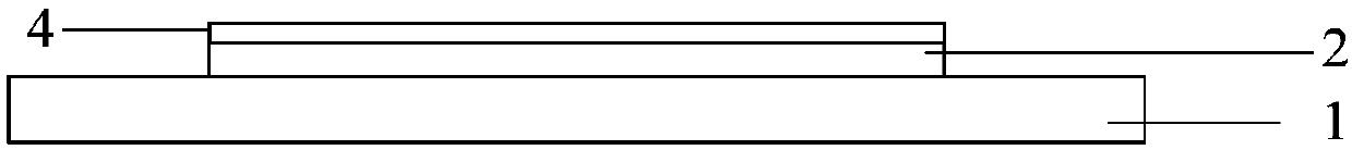
[0052] Next, a semiconductor pattern can b...
example 2
[0054] First, a gate and a gate insulating layer are formed on a glass substrate. Then, a first oxide semiconductor layer having a thickness of 30 nm was formed by deposition on the gate insulating layer. Here, ITZO is employed as the semiconductor oxide forming the first oxide semiconductor layer.
[0055] Then, a concentration of 10 wt% H 2 o 2 The solution is sprayed onto the surface of the first oxide semiconductor layer, and at the same time irradiated with ultraviolet light to promote the H 2 o 2 Decomposed into OH groups. The irradiation time of ultraviolet light is 2 minutes, and the irradiation intensity is 5000 nits.
[0056] Then, the H existing on the first oxide semiconductor layer 2 o 2 The solution was dried, and the second oxide semiconductor layer was deposited to a thickness of 15 nm in an oxygen-free atmosphere. Here, IGZO is employed as the semiconductor oxide forming the second oxide semiconductor layer.
[0057] Next, a semiconductor pattern can ...
example 3
[0059] First, a gate and a gate insulating layer are formed on a glass substrate. Then, a first oxide semiconductor layer having a thickness of 40 nm was formed by deposition on the gate insulating layer. Here, ZnO is employed as the semiconductor oxide forming the first oxide semiconductor layer.
[0060] Then, the concentration of 20 wt% H 2 o 2 The solution is sprayed onto the surface of the first oxide semiconductor layer, and at the same time irradiated with ultraviolet light to promote the H 2 o 2 Decomposed into OH groups. The irradiation time of ultraviolet light is 1 minute, and the irradiation intensity is 6000 nits.
[0061] Then, the H existing on the first oxide semiconductor layer 2 o 2 The solution was dried, and the second oxide semiconductor layer was deposited to a thickness of 10 nm in an oxygen-free atmosphere. Here, ZTO is employed as the semiconductor oxide forming the second oxide semiconductor layer.
[0062] Next, a semiconductor pattern can b...
PUM
| Property | Measurement | Unit |
|---|---|---|
| Thickness | aaaaa | aaaaa |
| Thickness | aaaaa | aaaaa |
| Thickness | aaaaa | aaaaa |
Abstract
Description
Claims
Application Information