Optical modulator

一种光调制器、相位调制的技术,应用在仪器、光学、非线性光学等方向,能够解决高频电信号损耗、无法大幅降低半导体的pn结或pin结部电阻值、无法降低Si半导体层203电阻值等问题,达到高效光调制、调制速度快、降低电阻值的效果

Active Publication Date: 2017-08-01
NIPPON TELEGRAPH & TELEPHONE CORP
View PDF3 Cites 10 Cited by
  • Summary
  • Abstract
  • Description
  • Claims
  • Application Information

AI Technical Summary

Problems solved by technology

In this way, there is a problem that the resistance value of the Si semiconductor layer 203 cannot be reduced by making the medium-concentration p-type semiconductor region 203-1 and the medium-concentration n-type semiconductor region 203-2 thick, and the phase inversion voltage Vπ cannot be reduced.
[0020] In addition, as described above, the doping concentration near the rib A0 (core of the optical waveguide) of the Si semiconductor layer 203 cannot be set to a high concentration, so the pn junction or pin junction of the semiconductor constituting the Si semiconductor layer 203 cannot be greatly reduced. resistance value
Therefore, there is also a problem that the resistance value of the Si semiconductor layer 203 causes high-frequency electrical signal loss, and the voltage applied to the pin junction or pn junction is attenuated, so that the phase inversion voltage Vπ cannot be reduced.

Method used


Image

  • Optical modulator
  • Optical modulator
  • Optical modulator

Examples


no. 1 approach

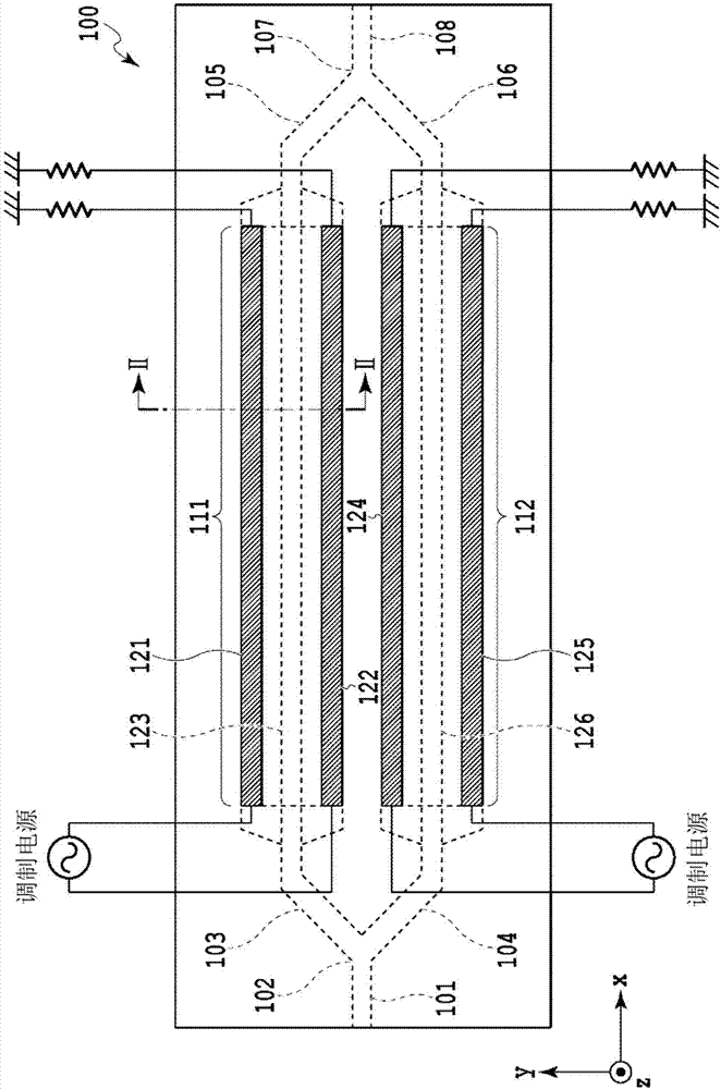
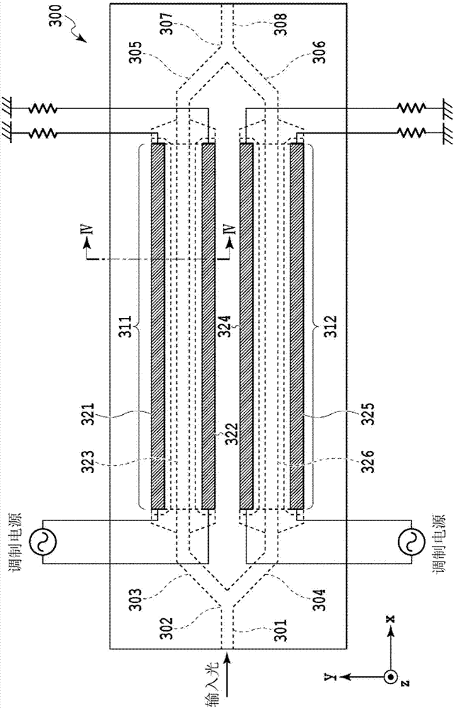
[0041] image 3 It is a top perspective view showing the configuration of the MZ-type optical modulator 300 according to the first embodiment of the present invention. The MZ type optical modulator 300 is a silicon optical modulator, equipped with: an input optical waveguide 301, an optical splitter 302 that splits the light incident from the input optical waveguide 301 1:1, and a light source from the optical splitter 302. The incident light guides 303 and 304 . In addition, the MZ-type optical modulator 300 includes: a phase modulator 311 that modulates the phase of light propagating through the optical waveguide 303; a phase modulator 312 that modulates the phase of light propagating through the optical waveguide 304; The optical waveguide 305 for the light of the phase modulator 311 and the optical waveguide 306 for transmitting the light from the phase modulator 312 . In addition, the MZ-type optical modulator 300 includes an optical multiplexer 307 for combining phase-...

Embodiment

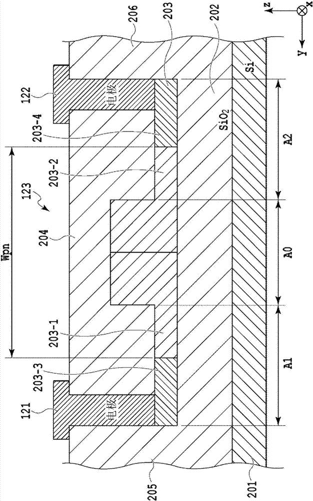
[0070] Based on the thickness t0 of the rib C0, the thickness t1 of the first flat portion C1, the thickness t2 of the second flat portion C2, the thickness t3 of the third flat portion C3, and the thickness t4 of the fourth flat portion C4 calculated as described above , the width w0 of the rib part C0, the width w1 of the first flat part C1, the width w2 of the second flat part C2, the width w3 of the third flat part C3, and the width w4 of the fourth flat part C4, as an example, the MZ type is formulated as follows Dimensions of the cross-sectional structure of the Si semiconductor layer 403 of the optical modulator 300 . Also, regarding the doping concentration, the settings are as follows.

[0071] Rib C0

[0072] t0=220nm w0=500nm

[0073] First flat part C1

[0074] t1=80nm w1=100nm

[0075] The second flat part C2

[0076] t2=80nm w2=100nm

[0077] The third flat part C3

[0078] t3=150nm w3>200nm

[0079] Fourth flat part C4

[0080] t4=150nm w4>200nm

[008...


PUM


Abstract

This optical modulator includes a substrate and a phase modulation unit on the substrate, said phase modulation unit including: a first traveling-wave electrode, a second traveling-wave electrode, and an optical waveguide configured from a first cladding layer, a semiconductor layer, which is laminated on the first cladding layer, and has a refractive index that is higher than that of the first cladding layer, and a second cladding layer, which is laminated on the semiconductor layer, and has a refractive index that is lower than that of the semiconductor layer. The semiconductor layer is provided with: a rib section, which is formed in the optical axis direction of the optical waveguide, and is to be the core of the optical waveguide; a first slab section formed in the optical axis direction on one side of the rib section; a second slab section formed in the optical axis direction on the other side of the rib section; a third slab section formed in the optical axis direction on the first slab section side opposite to the rib section; and a fourth slab section formed in the optical axis direction on the second slab section side opposite to the rib section. The first slab section is formed thinner than the rib section and the third slab section, and the second slab section is formed thinner than the rib section and the fourth slab section.

Description

technical field [0001] The invention relates to an optical modulator used in an optical communication system and an optical information processing system, in particular to a Mach-Zehnder type optical modulator which operates at low voltage and has small waveguide loss. Background technique [0002] The Mach-Zehnder type (MZ type) optical modulator has the following structure: the light incident on the optical waveguide is split into two waveguides through the optical splitter, and after the split light is propagated for a fixed length, it is passed through the optical combination oscillator to combine them again. Phase modulators are installed in the two optical waveguides that are branched to change the phase of the light transmitted to each optical waveguide, change the interference conditions of the combined light, and modulate the intensity or phase of the light. [0003] LiNbO is used as a material for the optical waveguide constituting the MZ-type optical modulator 3...

Claims


Application Information

Patent Timeline
Patent Type & Authority Applications(China)
IPC IPC(8): G02F1/025
CPCG02F1/2257G02F1/025G02F2201/063G02F2201/127G02F1/212
Inventor 都筑健龟井新地蔵堂真
Owner NIPPON TELEGRAPH & TELEPHONE CORP
Why Eureka
Try Eureka