Optic modulator and method of manufacturing the same

Active Publication Date: 2015-12-03
SK HYNIX INC +1
View PDF5 Cites 15 Cited by
  • Summary
  • Abstract
  • Description
  • Claims
  • Application Information

AI Technical Summary

Benefits of technology

[0015]In accordance with the embodiments of the present invention, the optic modulator may employ the modulation method based on the Schottky diode structure using a Schottky contact between metal and semiconductor. Thus, since the optic modulator has a rapid response characteristic, the optic modulator may effectively modulate an electrical signal having a high frequency into an optical signal.
[0016]Furthermore, since ITO which can perform a high-speed operation and is optically transparent is employed as a conductive material, ITO may have a small influence on an optical conf

Problems solved by technology

Thus, it takes a long time to supply/discharge carriers.
Furthermore, the switching type of the P-I-N diode structure is limited.
In particular, it tak

Method used


Image

  • Optic modulator and method of manufacturing the same
  • Optic modulator and method of manufacturing the same
  • Optic modulator and method of manufacturing the same

Examples


Example

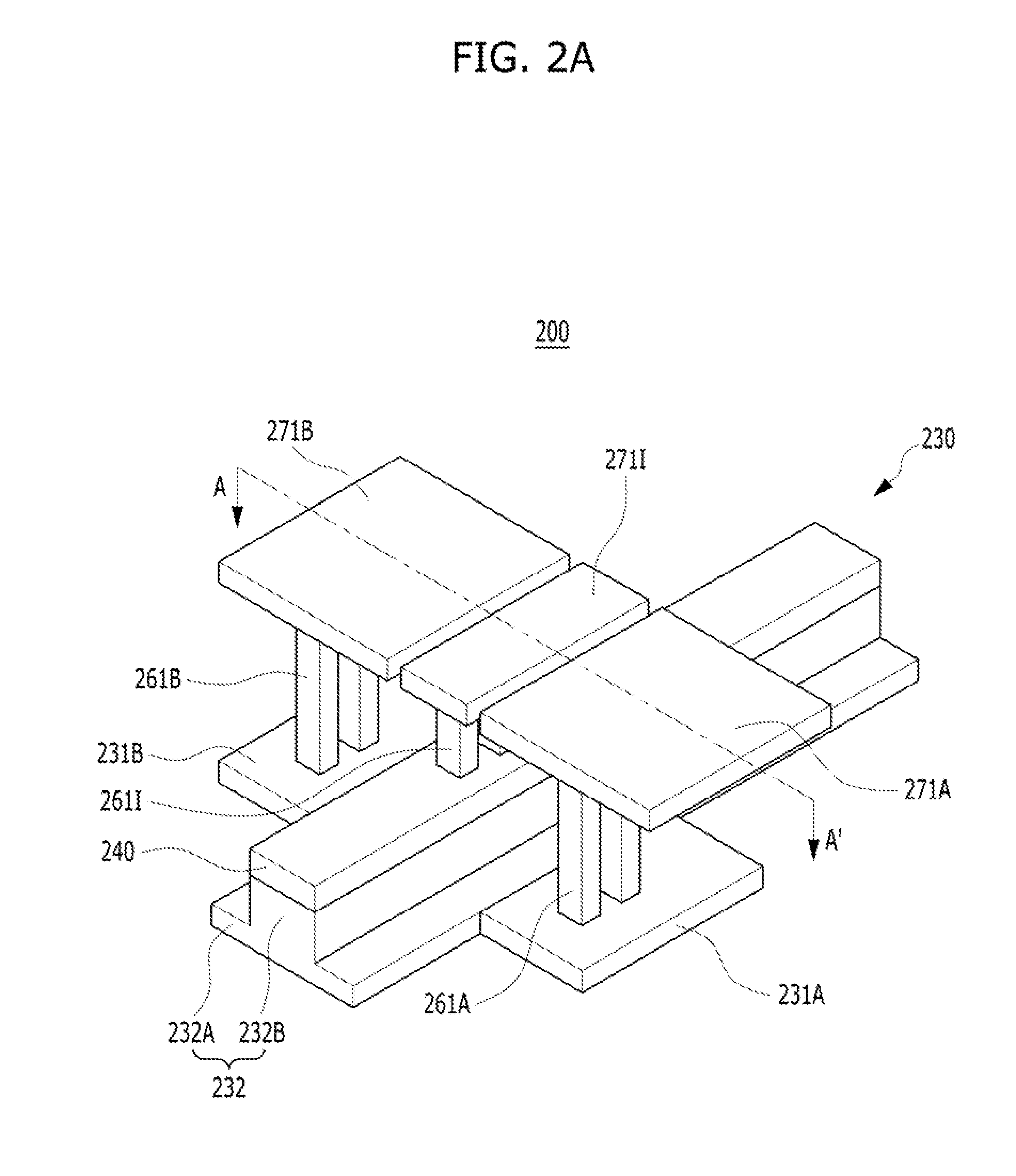
[0029]FIG. 2A is a perspective view of an optic modulator in accordance with a first embodiment. FIG. 2B is a cross-sectional view of the optic modulator, taken along like A-A′ of FIG. 2A.

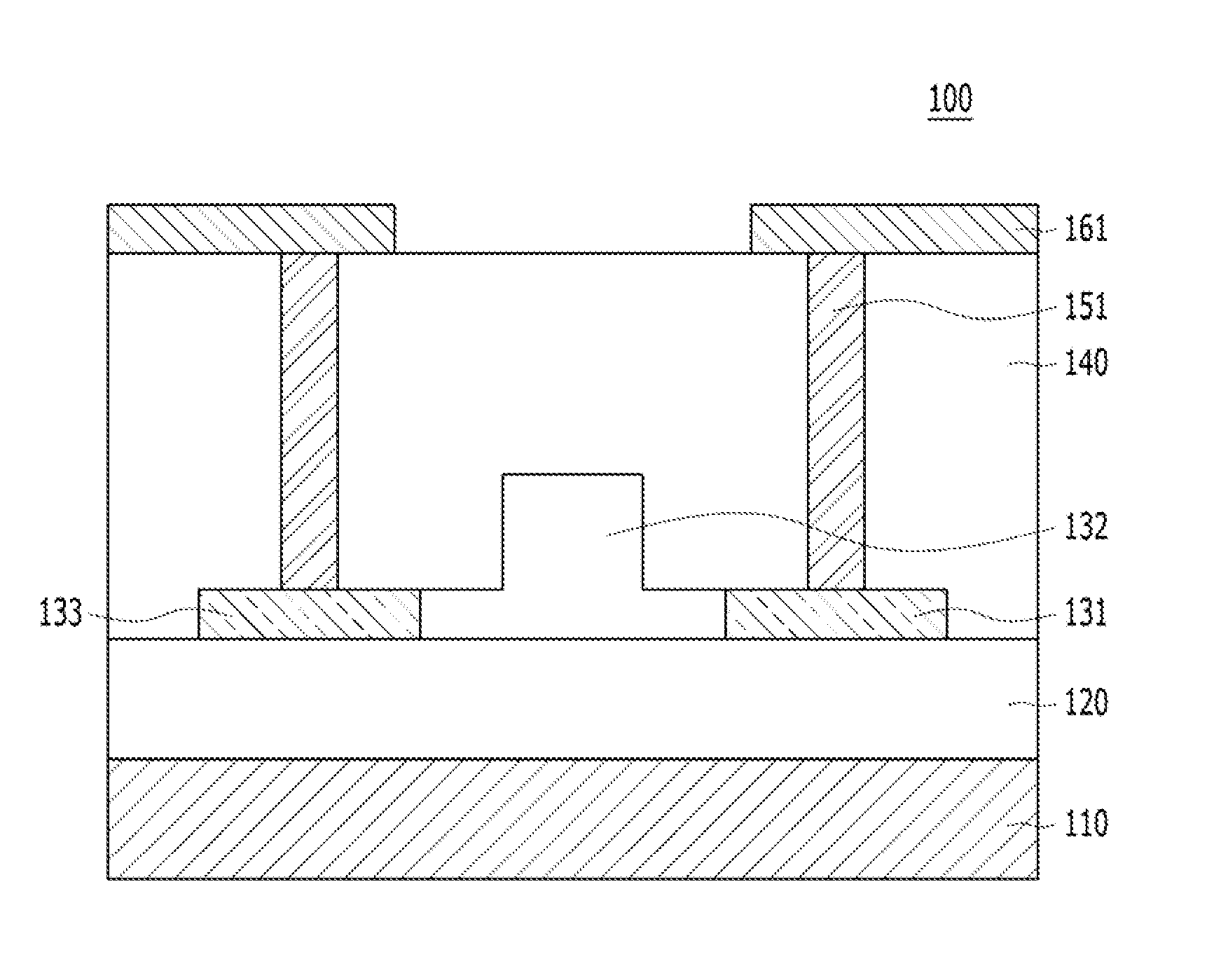
[0030]Referring to FIGS. 2A and 2B, the optic modulator 200 in accordance with the present embodiment may be formed over a semiconductor substrate 210. The semiconductor substrate 210 may include a material suitable for semiconductor processing. The semiconductor substrate 210 may contain silicon. For example, the semiconductor substrate 210 may include a silicon substrate. In another embodiment, the semiconductor substrate 210 may include a single-crystal silicon substrate. The semiconductor substrate 310 may include a SiGe substrate. The semiconductor substrate 210 may include a compound semiconductor such as GaAs or InP.

[0031]An insulating layer 220 may be formed over the semiconductor substrate 210. The insulating layer 220 may include silicon oxide. The insulating layer 220 may be formed throu...

Example

[0043]FIG. 3 is a diagram illustrating an optic modulator in accordance with a second embodiment.

[0044]In the present embodiment, the optic modulator 300 may be formed over a semiconductor substrate 310. The semiconductor substrate 310 may include a material suitable for semiconductor processing. The semiconductor substrate 310 may contain silicon. For example, the semiconductor substrate 310 may include a silicon substrate. In another embodiment, the semiconductor substrate 310 may include a single-crystal silicon substrate. The substrate 310 may include a SiGe substrate. The semiconductor substrate 310 may include a compound semiconductor such as GaAs or InP.

[0045]An insulating layer 320 may be formed over the semiconductor substrate 310. The insulating layer 320 may include silicon oxide. The insulating layer 320 may be formed through oxidation or deposition. The insulating layer 320 may serve to optically separate the semiconductor substrate 310 and an optical waveguide 230 from...

Example

[0060]FIG. 4 is a diagram illustrating an optic modulator in accordance with a third embodiment.

[0061]The third embodiment does not disclose an optic modulator having a Schottky diode structure, but discloses an optic modulator using a metal-insulator-semiconductor capacitor structure.

[0062]In the present embodiment, the optic modulator 400 may be formed over a semiconductor substrate 410. The semiconductor substrate 410 may include a material suitable for semiconductor processing. The semiconductor substrate 410 may contain silicon. For example, the semiconductor substrate 410 may include a silicon substrate. In another embodiment, the semiconductor substrate 410 may include a single-crystal silicon substrate. The substrate 410 may include a SiGe substrate. The semiconductor substrate 410 may include a compound semiconductor such as GaAs or InP.

[0063]An insulating layer 420 may be formed over the semiconductor substrate 410. The insulating layer 420 may include silicon oxide. The i...


PUM


Abstract

An optic modulator may include: an optical waveguide including a ridge-shaped portion having a first region and a second region over the first region; a slab-shaped portion being in contact with a first region of the ridge-shaped portion; an optical waveguide electrode forming a Schottky contact with a second region of the ridge-shaped portion; metal plugs being in contact with the slab-shaped portion and the optical waveguide electrode, respectively; and metal pads connected to the respective metal plugs.

Description

BACKGROUND[0001]1. Technical Field[0002]Exemplary embodiments of the present invention relate to an optical device, and more particularly, to an optic modulator.[0003]2. Related Art[0004]Recently, with the increase in signal processing speed of integrated circuits, much research has been conducted on a method for implementing communications between semiconductor chips using optical signals. A core element of an optical integrated circuit for processing such optical signals is an electro-optic modulator. The electro-optic modulator generates an optical signal by modulating a constant intensity of light emitted from an external internal light source.[0005]The optic modulator within the optical integrated circuit performs a function of converting an electrical signal into an optical signal. In order to perform such a function, the optic modulator uses an electro-optic effect. In particular, a semiconductor material such as silicon may have an effective refractive index which changes du...

Claims


Application Information

Patent Timeline
IPC IPC(8): G02F1/025H01L29/47H01L29/417H01L29/872
CPCG02F1/025H01L29/417H01L29/47H01L29/872G02F1/011G02B2006/12123G02B2006/12142G02B6/12
Inventor LEE, JONG-HOYOO, KEON
Owner SK HYNIX INC
Why Eureka
Try Eureka