Semiconductor optical modulator, an optical amplifier and an integrated semiconductor light-emitting device

a semiconductor light-emitting device and optical modulator technology, applied in the direction of semiconductor amplifiers, semiconductor lasers, instruments, etc., can solve the problems of severe degradation of the s/n ratio of optical modulation, affecting the performance of optical modulation, and affecting the efficiency of optical modulation

Inactive Publication Date: 2006-03-16
TAKAHASHI TAKASHI +1
View PDF25 Cites 73 Cited by
  • Summary
  • Abstract
  • Description
  • Claims
  • Application Information

AI Technical Summary

Benefits of technology

[0012] Accordingly, it is a general object of the present invention to provide a novel and useful optical semiconductor device and a fabrication pro

Problems solved by technology

However, conventional EA-type semiconductor optical modulator that uses the InP/InGaAsP multiple quantum well structure has a drawback, due to the relatively small conduction band discontinuity between the InP barrier layer and the InGaAsP quantum well layer, in that the excitons are tend to be destroyed due to the leakage of electrons from the quantum well layer upon application of the voltage to the quantum well layer, wherein this problem becomes particularly serious when operating the EA modulator at high temperatures.
As a result, there arises a problem of severe degradation of S/N ratio of optical modulation.
In such a system, however, there arises a problem similar to the case of the EA-type optical modulator in that, because of the relatively small conduction band discontinuity between the InGaAsP layer acting as the gain region and the InP layer acting as

Method used


Image

  • Semiconductor optical modulator, an optical amplifier and an integrated semiconductor light-emitting device
  • Semiconductor optical modulator, an optical amplifier and an integrated semiconductor light-emitting device
  • Semiconductor optical modulator, an optical amplifier and an integrated semiconductor light-emitting device

Examples


embodiment 1

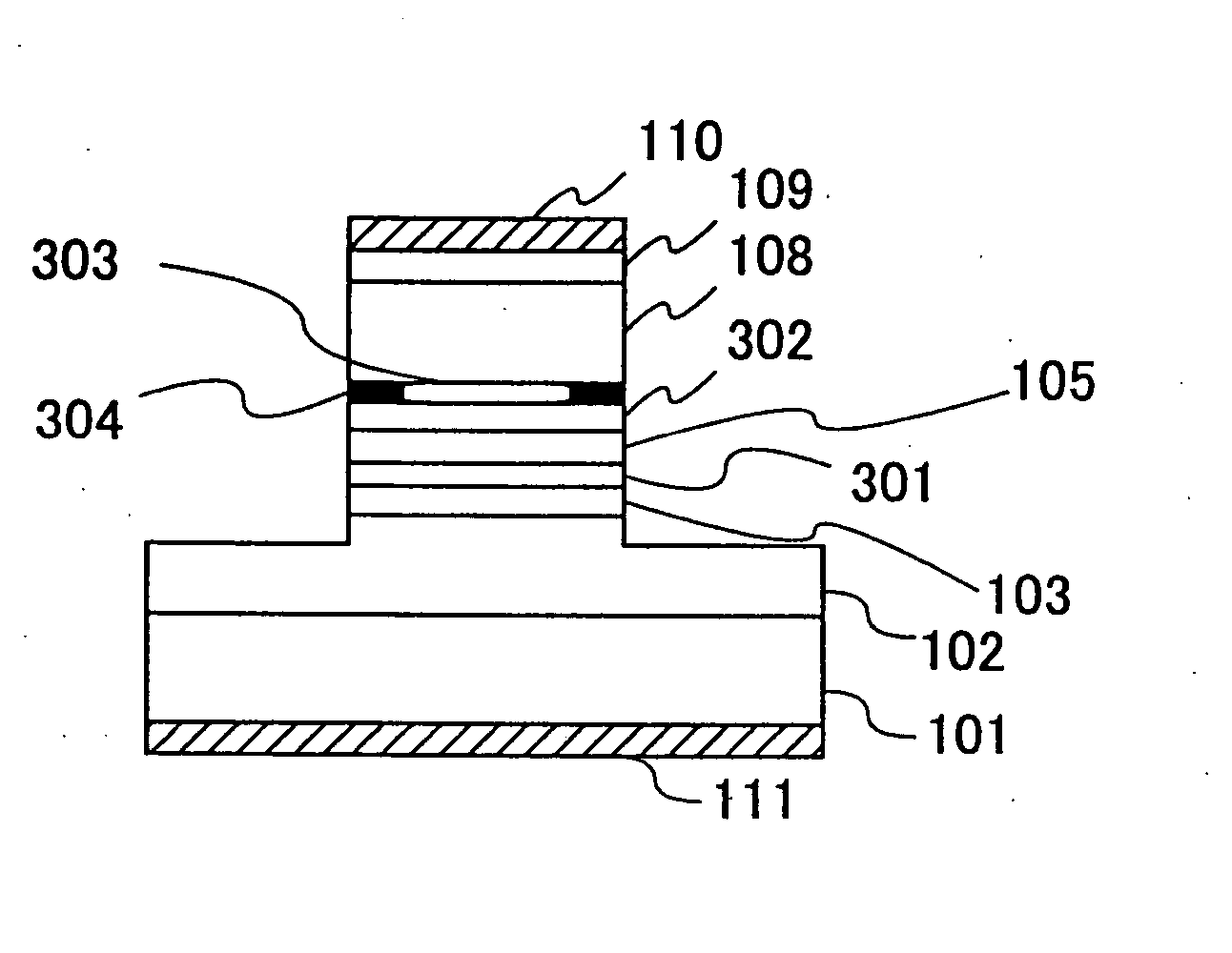
[0056]FIGS. 1A and 1B show the construction of a semiconductor optical modulator according to Embodiment 1 of the present invention, wherein FIG. 1A shows the semiconductor optical modulator in a front end view while FIG. 1B shows the semiconductor optical modulator in a longitudinal cross-sectional view.

[0057] Referring to FIGS. 1A and 1B, the semiconductor optical modulator is constructed on an n-type GaAs substrate 101 and includes a lower cladding layer 102 of n-type AlGaAs having a composition of Al0.4Ga0.6As and grown epitaxially on the substrate 101, a lower optical waveguide layer 103 of GaAs grown epitaxially on the cladding layer 102 and a multiple quantum well structure 301 grown epitaxially on the lower optical waveguide layer 103.

[0058] On the multiple quantum well structure 301, an upper optical waveguide layer 105 of GaAs is grown epitaxially, and a first upper cladding layer 302 of p-type AlGaAs having a composition represented as Al0.4Ga0.6As, a p-type AlAs select...

embodiment 2

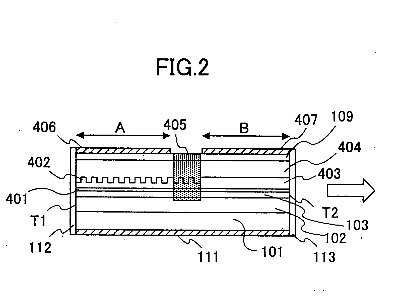
[0086]FIG. 2 shows the construction of an integrated semiconductor light-emitting device according to Embodiment 2 of the present invention.

[0087] Referring to FIG. 2, the integrated semiconductor light-emitting device is a laser diode device having an integral optical modulator, and includes a laser diode part A that produces a laser beam and an EA-type semiconductor optical modulator B that modulates the intensity of the optical beam produced by the laser diode part A, such that the laser diode part A and the semiconductor optical modulator B are integrated on the n-type GaAs substrate 101 commonly and monolithically.

[0088] Here, it should be noted that the laser diode part A includes the n-type AlGaAs layer 102 having the composition of Al0.4Ga0.6As as a cladding layer, the GaAs layer 103 as a lower optical waveguide layer, and a multiple quantum well structure 401 is formed on the lower optical waveguide layer 103. Further, a diffraction grating layer 402 and a p-type cladding...

embodiment 3

[0106]FIGS. 3A and 3B show another construction of the integrated semiconductor light-emitting device according to Embodiment 3 of the present invention, wherein FIG. 3A shows the device in a plan view while FIG. 3B shows the device in a longitudinal cross-sectional view.

[0107] Referring to FIGS. 3A and 3B, the integrated semiconductor light-emitting device is constructed on a Si substrate 1001 and includes a vertical-cavity surface-emission laser diode 1002 formed on the Si substrate 1001, wherein there are provided four such laser diodes 1002 on the substrate 1001 in the form of an array. Further, the Si substrate 1001 carries thereon an optical waveguide 1004 having a 45° mirror 1003 at an end thereof, and an EA-type semiconductor optical modulator 1005 is provided further on the Si substrate 1001 in optical coupling with the other end of the optical waveguide 1004. The EA-type semiconductor optical modulator 1005 includes four channels, and optical fibers 1006 are coupled to re...


PUM


Abstract

An integrated semiconductor optical-emitting device includes a surface-emission laser diode and an EA-type semiconductor optical modulator integrated commonly on a GaAs substrate in a direction perpendicular to the GaAs substrate.

Description

BACKGROUND OF THE INVENTION [0001] The present invention generally relates to optical semiconductor devices. Especially, it is related to optical semiconductor devices such as a semiconductor optical modulator, a semiconductor light-emitting device, a semiconductor optical amplifier, an optical source of amplitude spontaneous emission (ASE), an optical gate array, a tunable laser apparatus, a multi-wavelength laser apparatus, and also an optical transmission system that uses such an optical semiconductor device. Further, the present invention relates to the fabrication process of the optical semiconductor devices. [0002] Japanese Laid-Open Patent Publication 10-22805 describes a semiconductor optical modulator that uses an InGaAsP multiple quantum well structure. In this reference, an InP / InGaAsP multiple quantum well structure is used as an optical modulator, and optical modulation is achieved by causing quantum confinement Stark effect in the multiple quantum well structure. In qu...

Claims


Application Information

Patent Timeline
IPC IPC(8): H01L33/00G02F1/017H01S5/026H01S5/10H01S5/183H01S5/323H01S5/40H01S5/50
CPCB82Y20/00H01S2301/173G02F1/01708H01S5/0265H01S5/101H01S5/1085H01S5/18302H01S5/18305H01S5/18308H01S5/18311H01S5/18358H01S5/32366H01S5/34306H01S5/4012H01S5/4087H01S5/50G02F1/017
Inventor TAKAHASHI, TAKASHISATO, SHUNICHI
Owner TAKAHASHI TAKASHI
Why Eureka
Try Eureka