

Machining method for polishing process of RB-SiC optical element
A technology for optical components and process processing, which is applied in the direction of optical surface grinders, metal processing equipment, grinding/polishing equipment, etc., can solve the problems of low processing efficiency, low magnetron sputtering deposition rate, long processing time, etc., to achieve The effect of improving processing efficiency, shortening processing cycle, and shortening processing cycle
- Summary
- Abstract
- Description
- Claims
- Application Information
AI Technical Summary
Problems solved by technology
Method used
Image

Examples
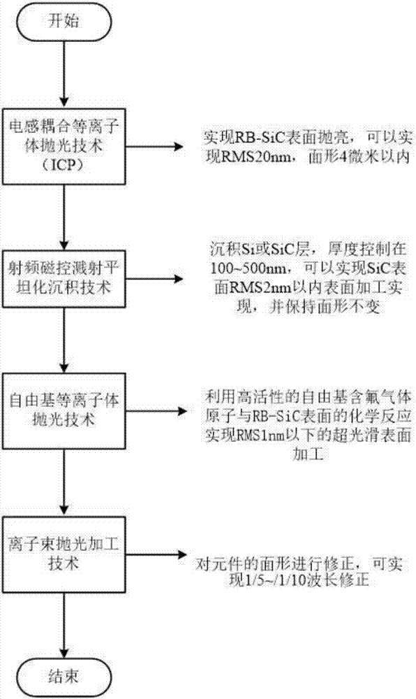
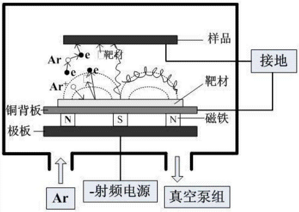
Embodiment 1
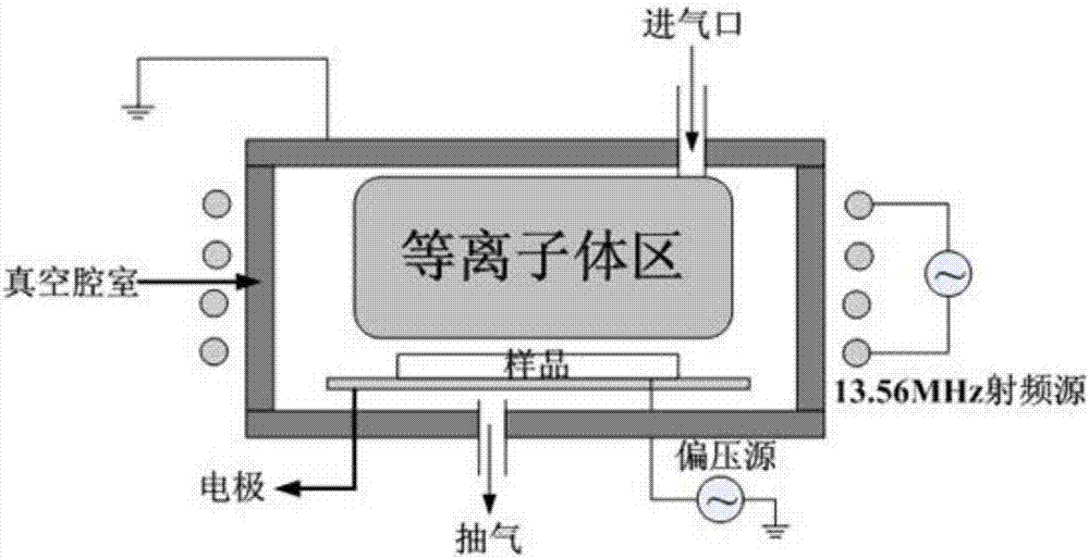
[0064] 1) ICP etching: see figure 2 , The background vacuum of the vacuum chamber of the ICP etching equipment is 2.0×10 -4 Pa, the working vacuum is controlled at 0.5~10Pa. Put the reaction sintered silicon carbide sample (RMS at 209.72nm) with a diameter of 150mm and a thickness of 10mm on the base of the vacuum chamber of the ICP etching equipment, and open the pre-pumping valve and the front-stage valve in sequence. When the pressure value of the composite vacuum gauge drops to At 5Pa, turn on the molecular pump, press the start button, wait until the molecular pump speed reaches 400r / min, open the high valve, and close the pre-pumping valve at the same time, when the pressure value of the composite vacuum gauge is lower than 10 -1 At Pa, set the gas flow meter to CF 4 Turn the switch of the gas flowmeter to the valve control position, adjust the knob of the flowmeter, set the flow rates of the two gases to 25sccm respectively, then open the main gas valve, adjust the h...
PUM
| Property | Measurement | Unit |
|---|---|---|
| surface roughness | aaaaa | aaaaa |
| surface roughness | aaaaa | aaaaa |
| surface roughness | aaaaa | aaaaa |
Abstract
Description
Claims
Application Information