Method for reducing silicon carbide epitaxial basal plane dislocation density

A silicon carbide, basal plane technology, applied in electrical components, semiconductor/solid-state device manufacturing, circuits, etc., can solve the problems of inappropriate silicon carbide epitaxy process, cumbersome process, surface damage of silicon carbide substrate, etc., to reduce BPD defects , avoid pre-processing, reduce the effect of damage

Active Publication Date: 2017-08-18
NO 55 INST CHINA ELECTRONIC SCI & TECHNOLOGYGROUP CO LTD
View PDF4 Cites 23 Cited by
  • Summary
  • Abstract
  • Description
  • Claims
  • Application Information

AI Technical Summary

Problems solved by technology

However, KOH melting corrosion or KOH–NaOH–MgO eutectic corrosion of silicon carbide substrates seriously damages the surface of silicon carbide substrates, and the process is relatively cumbersome, which is not suitable for silicon carbide epitaxy process integration.

Method used


Image

  • Method for reducing silicon carbide epitaxial basal plane dislocation density
  • Method for reducing silicon carbide epitaxial basal plane dislocation density
  • Method for reducing silicon carbide epitaxial basal plane dislocation density

Examples


Embodiment 1

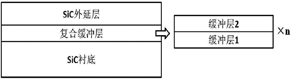
[0035] To grow a SiC epitaxial wafer on a composite buffer layer with a periodic high-low doping structure, the specific steps are as follows:

[0036] (1) Select a silicon carbide substrate with a silicon surface that is 4° to the direction, and the substrate BPD defect density is 1000cm -2 ,, the substrate is placed in the reaction chamber of the SiC epitaxial system, placed on the graphite base, and the graphite base has a tantalum carbide coating;

[0037] (2) Use argon to replace the gas in the reaction chamber several times, introduce hydrogen into the reaction chamber, and gradually increase the H 2 Flow rate to 80L / min, set the pressure of the reaction chamber to 100mbar, gradually raise the temperature of the reaction chamber to the growth temperature of 1600°C, maintain the temperature of the reaction chamber for 10 minutes after reaching the growth temperature, and perform pure hydrogen etching on the substrate;

[0038](3) A small flow of silane (SiH 4 ) and pro...

Embodiment 2

[0045] To grow SiC epitaxial wafers on a composite buffer layer with two periods of high-low doping structure, the specific steps are as follows:

[0046] (1) Select a silicon carbide substrate with a silicon surface that is 4° to the direction, and the substrate BPD defect density is 1000cm -2 ,, the substrate is placed in the reaction chamber of the SiC epitaxy system, placed on the graphite base, and the graphite base has a tantalum carbide coating;

[0047] (2) Use argon to replace the gas in the reaction chamber several times, introduce hydrogen into the reaction chamber, and gradually increase the H 2 Flow rate to 80L / min, set the pressure of the reaction chamber to 100mbar, gradually raise the temperature of the reaction chamber to the growth temperature of 1600°C, maintain the temperature of the reaction chamber for 10 minutes after reaching the growth temperature, and perform pure hydrogen etching on the substrate;

[0048] (3) A small flow of silane (SiH 4 ) and p...


PUM


Abstract

The invention discloses a method for reducing silicon carbide epitaxial basal plane dislocation density. The method comprises the steps of epitaxially growing a composite buffer layer of high-low doping concentration of multiple cycles on a SiC substrate, carrying out interface high temperature hydrogen etching processing on each single buffer layer, using interface high temperature processing and doping induction to introduce multiple interfaces, and using an interface image force to promote the conversion of a BPD defect to a TED defect. According to the method, the BPD defect in an epitaxial layer is greatly reduced, the BPD defect density in an epitaxial layer can be effectively reduced, the method is simple and the integration of epitaxial process is facilitated, at the same time the complex preprocessing of the SiC substrate is avoided, and the damage to the surface of the substrate is reduced.

Description

technical field [0001] The invention relates to a method for growing a silicon carbide epitaxial layer, in particular to a method for reducing the plane dislocation density of a silicon carbide epitaxial base. Background technique [0002] The commercialization of silicon carbide power electronics is mainly limited by the structural defects in the silicon carbide epitaxial layer. The structural defects will lead to the degradation of the performance of silicon carbide devices, which will lead to a decrease in breakdown voltage, reduce the lifetime of minority carriers, and increase the forward conduction resistance. The long-term goal of silicon carbide research is to eliminate these defects. [0003] The main problem in the current research on silicon carbide devices is to solve the stacking faults caused by the induced recombination in the active region of the device under forward bias. Stacking faults lead to degradation of device performance over time, increasing turn-o...

Claims


Application Information

Patent Timeline
IPC IPC(8): H01L21/02H01L21/3065
CPCH01L21/02008H01L21/02436H01L21/02612H01L21/3065H01L21/02378H01L21/02447H01L21/02507H01L21/02529H01L21/0262H01L21/02293
Inventor 李赟
Owner NO 55 INST CHINA ELECTRONIC SCI & TECHNOLOGYGROUP CO LTD
Why Eureka
Try Eureka