Thin film solar cell and preparation method thereof

A solar cell and thin film technology, applied in circuits, electrical components, photovoltaic power generation, etc., can solve the problems of high manufacturing cost, difficulty in large-scale production, and increased material cost, and achieve simple production and equipment, easy large-scale production, and reduced The effect of material cost

Inactive Publication Date: 2017-08-18
CHONGQING UNIV OF ARTS & SCI
View PDF5 Cites 12 Cited by
  • Summary
  • Abstract
  • Description
  • Claims
  • Application Information

AI Technical Summary

Problems solved by technology

[0006] Among them, the first vacuum deposition will undoubtedly increase the Sb 2 Se 3 The equipment cost and production cycle of thin-film solar cells, and the size is limited by the degree of vacuum and the cavity, large-scale production is difficult, and the manufacturing cost is high
[0007] In the second method, hydrazine hydrate will cause incalculable damage to people and the environment, so it is not suitable to use Sb 2 Se 3 Production of thin film solar cells
[0008] Furthermore, since Sb 2 S 3 (Se) or Sb 2 Se 3 The bonding force of thin film and cheap common metal electrodes such as Ag is poor, and Sb in the prior art 2 S 3 (Se) or Sb 2 Se 3 The anode of solar cells usually uses noble metal Au as the electrode, which significantly increases the material cost and further limits its application.

Method used


Image

  • Thin film solar cell and preparation method thereof
  • Thin film solar cell and preparation method thereof
  • Thin film solar cell and preparation method thereof

Examples


Embodiment 1

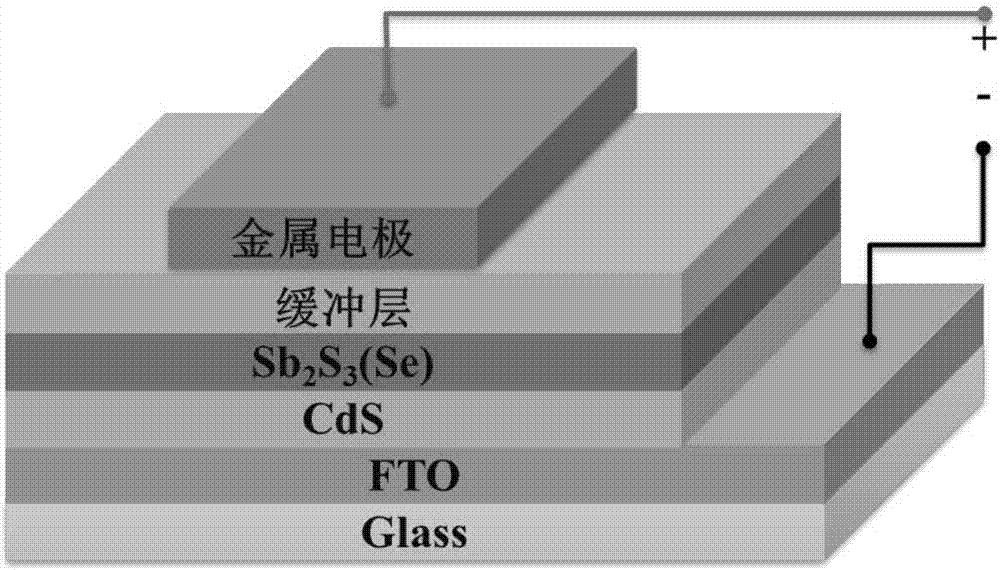
[0036]Thin film solar cells are basically as attached figure 1 as shown,

[0037] a Sb 2 S 3 The bottom layer of the structure of (Se) thin film solar cells is the substrate, and above the substrate are FTO, CdS, Sb 2 S 3 (Se), MoO 3 , Ag, the preparation steps are as follows:

[0038] (1) Substrate cleaning

[0039] Clean the FTO / glass substrate in deionized water, acetone, and isopropanol for 10 minutes with an ultrasonic cleaner, and then dry it.

[0040] (2) CdS film deposition

[0041] Thiourea and CdCl 2 Soluble in H 2 O, adding a certain amount of NH 4 ·H 2 O, CdCl 2 The concentration is 1.2mmol / L, thiourea and CdCl 2 The ratio of the amount of substance is: 100:7.2; NH 4 ·H 2 O is used to adjust the pH value of the solution to 11.5, the temperature of the water bath is 80° C., the deposition time is 30 min, and the thickness of CdS is 120 nm.

[0042] (3) Deposition of Sb on CdS film 2 S 3 (Se) thin film

[0043] i. Solution configuration

[0044] S...

Embodiment 2

[0055] The difference from Example 1 is: Sb in the precursor solution 3+ The concentration is 0.5mol / L, Sb 2 S 3 The film thickness is 500nm, the thickness of CdS is 150nm, and the buffer layer material is MoO 3 , MoO 3 The thickness is 3nm, the material of the metal electrode is Au, and the thickness of the metal electrode is 60nm. In step 3, the temperature at the high temperature end of selenization is controlled at 380°C, the temperature at the low temperature end is controlled at 350°C, and the selenization time is 5min.

Embodiment 3

[0057] The difference from Example 1 is: Sb in the precursor solution 3+ The concentration is 0.4mol / L, Sb 2 S 3 The thickness of the film is 1500nm, the thickness of CdS is 100nm, the material of the buffer layer is NiO, the thickness of NiO is 15nm, the material of the metal electrode is Pt, and the thickness of the metal electrode is 80nm. The temperature is controlled at 350°C, and the selenization time is 13 minutes.


PUM

PropertyMeasurementUnit
thicknessaaaaaaaaaa
thicknessaaaaaaaaaa
thicknessaaaaaaaaaa

Abstract

The present invention belongs to the inorganic nonmetallic material science and photoelectric film and device manufacturing field, and especially discloses to a thin film solar cell and a preparation method thereof. The structure of a thin film solar cell is FTO/CdS/Sb2S3 (Se)/a buffer layer/a metal electrode, wherein the buffer layer is p-type transition metallic oxide and includes but not limited to WO3, MoO3, NiO, CoO and the like, and the metal electrode is a high-work-function metal and includes but not limited to Ag, Au, Pt and the like. The preparation steps comprises: (1) cleaning of the substrate; (2) deposition of the CdS film; (3) preparation of the Sb2S3 (Se) film; and (4) deposition of the buffer layer and the metal electrode. The objective of the invention is to provide Sb2S3(Se) thin film solar cell based on new materials and a new structure, and a technology with low cost and capable of preparing the large-area Sb2S3(Se) thin film and the solar cell.

Description

technical field [0001] The invention relates to a low-cost, non-toxic thin-film solar battery and a preparation method thereof, belonging to the fields of inorganic non-metallic material science and photoelectric thin film and device manufacturing. Background technique [0002] Inorganic thin-film solar cells have the advantages of high conversion efficiency, low price, light and thin, etc., and have broad application prospects. At present, the existing thin-film solar cell absorber materials usually contain high levels of toxic elements and rare elements, such as cadmium telluride solar cells contain toxic element cadmium and rare element tellurium, copper indium gallium selenide solar cells contain rare and expensive elements indium, gallium , which largely limits their large-scale production and long-term use. Therefore, it is the future trend of solar cell development to use semiconductor materials with wide sources, low price, green and non-toxic as solar cell material...

Claims


Application Information

Patent Timeline
Patent Type & Authority Applications(China)
IPC IPC(8): H01L31/072H01L31/0445H01L31/0336H01L31/18
CPCH01L31/0336H01L31/0445H01L31/072H01L31/18Y02E10/50Y02P70/50
Inventor 程江李璐廖小青胡荣杨鑫
Owner CHONGQING UNIV OF ARTS & SCI
Why Eureka
Try Eureka