
Confocal microscope parallel scanning device and scanning method based on scanning galvanometer and semiconductor laser

A technology of confocal microscope and scanning galvanometer, which is applied in microscopes, optics, instruments, etc., can solve the problems of exposure speed influence, low image acquisition rate, etc., and achieve the effect of increasing scanning speed and improving acquisition speed

Active Publication Date: 2017-08-22
HARBIN INST OF TECH
View PDF8 Cites 9 Cited by
  • Summary
  • Abstract
  • Description
  • Claims
  • Application Information

AI Technical Summary

Problems solved by technology

[0009] The present invention is to solve the problem that the existing CCD camera is affected by the exposure speed and the picture acquisition rate is low. The present invention provides a confocal microscope parallel scanning device and scanning method based on scanning galvanometer and semiconductor laser

Method used


Image

  • Confocal microscope parallel scanning device and scanning method based on scanning galvanometer and semiconductor laser
  • Confocal microscope parallel scanning device and scanning method based on scanning galvanometer and semiconductor laser
  • Confocal microscope parallel scanning device and scanning method based on scanning galvanometer and semiconductor laser

Examples


specific Embodiment approach 1

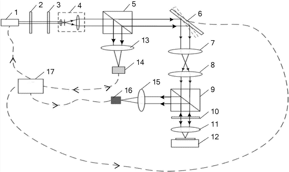
[0025] Specific implementation mode one: see figure 1 Describe this embodiment, a confocal microscope parallel scanning device based on a scanning galvanometer and a semiconductor laser described in this embodiment, it includes a semiconductor laser 1, an attenuation plate 2, a polarizer 3, a collimating beam expander system 4, a first A polarizing beam splitting prism 5, scanning galvanometer system 6, telecentric scanning lens 7, tube mirror 8, second polarizing beam splitting prism 9, 1 / 4 wave plate 10, objective lens 11, first collecting lens 13, photodetector 14, Second collecting lens 15, CCD camera 16 and controller 17;

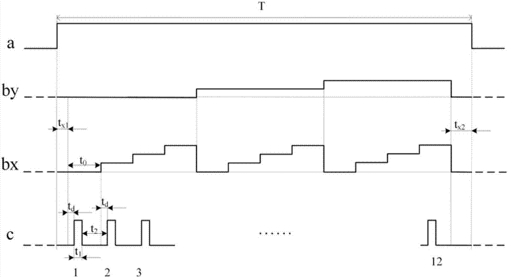
[0026] The controller 17 is used for modulating the outgoing light of the semiconductor laser 1, for controlling the photodetector 14 to perform photodetection, for controlling the exposure time of the CCD camera 16, and for controlling the scanning galvanometer system 6 to deflect;

[0027] The light emitted by the semiconductor laser 1 is transmitte...

specific Embodiment approach 2

[0040] Specific implementation mode two: see figure 1 Describe this embodiment, the difference between this embodiment and the confocal microscope parallel scanning device based on the scanning galvanometer and semiconductor laser described in the first embodiment is that the 1 / 4 wave plate 10 is incident on the objective lens 11 The light is circularly polarized.

specific Embodiment approach 3

[0041] Specific implementation mode three: see figure 1 Describe this embodiment, the difference between this embodiment and the confocal microscope parallel scanning device based on the scanning galvanometer and semiconductor laser described in the first embodiment is that the 1 / 4 wave plate 10 is incident to the second The light from the polarization beam splitter prism 9 is linearly polarized light.


PUM


Abstract

The invention provides a confocal microscope parallel scanning device and scanning method based on a scanning galvanometer and a semiconductor laser, belongs to the field of confocal microscopy imaging, and solves the problem of low image acquisition rate of a conventional CCD camera due to the influence of the exposure speed. The device comprises the semiconductor laser, an attenuator, a polaroid, a collimation beam-expanding system, a first polarization beam-splitting prism, a scanning galvanometer system, a telecentric scanning lens, a tubular lens, a second polarization beam-splitting prism, a quarter-wave plate, an objective lens, a first collection lens, a photoelectric detector, a second collection lens, a CCD camera and a controller. According to the device and method, the exposure time of the CCD camera in a confocal optical path is modulated, the scanning galvanometer system and the semiconductor laser trigger signals, laser spots corresponding to a plurality of galvanometer deflection angles are obtained on one frame of image of the CCD camera, parallel scanning is realized, and the device and method can be mainly used for scanning samples.

Description

technical field [0001] The invention belongs to the field of confocal microscopic imaging. Background technique [0002] Optical microscopy is widely used in fields such as biology and materials science. Confocal microscopic measurement technology is a three-dimensional optical microscopy technology suitable for micron and submicron scale measurement. The tomographic capabilities of reflective confocal microscopy systems make them important in the field of 3D imaging. [0003] The confocal microscope was invented by Minsky in the mid-to-late 1950s. In 1977, C.J.R.Sheppard and A.Choudhury clarified that the confocal microscope system, under the action of a point pinhole mask, sacrificed the field of view to increase the lateral resolution to the same aperture as ordinary microscopes 1.4 times. However, due to the introduction of conjugate pinholes, the traditional confocal technology can only detect one point at a time, and requires scanning to realize the three-dimensiona...

Claims


Application Information

Patent Timeline
IPC IPC(8): G02B21/00
CPCG02B21/0032G02B21/0036G02B21/0068
Inventor 倪赫郭清源严情邹丽敏张鹏
Owner HARBIN INST OF TECH
Learn More