3D photonic integration with light coupling elements

A technology of optical coupling and grating coupler, which is applied in the direction of optical components, optical waveguide coupling, electrical components, etc.

Inactive Publication Date: 2017-08-29
BIOND PHOTONICS
View PDF3 Cites 42 Cited by
  • Summary
  • Abstract
  • Description
  • Claims
  • Application Information

AI Technical Summary

Problems solved by technology

Although the wafer bonding method allows efficient implementation of scalability (i.e., increased number of lasers on a Si chip), it requires fabri

Method used


Image

  • 3D photonic integration with light coupling elements
  • 3D photonic integration with light coupling elements
  • 3D photonic integration with light coupling elements

Examples


Embodiment Construction

[0049] The systems, devices and methods described herein should not be construed as limiting in any way. On the contrary, the present disclosure is directed to all novel and non-obvious features and aspects of the various disclosed embodiments individually and in various combinations and subcombinations with each other. The disclosed systems, methods and apparatus are not limited to any particular aspect or feature or combination thereof, nor do the disclosed systems, methods and apparatus require the existence of any one or more particular advantages or problems to be solved. Any theories of operation are presented for convenience of explanation, but the disclosed systems, methods and devices are not limited to these theories of operation.

[0050] Although the operations of some disclosed methods are described in a particular sequential order for convenience of presentation, it should be understood that such description includes rearrangements unless specific language set fo...


PUM


Abstract

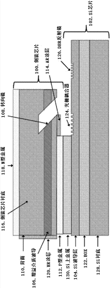
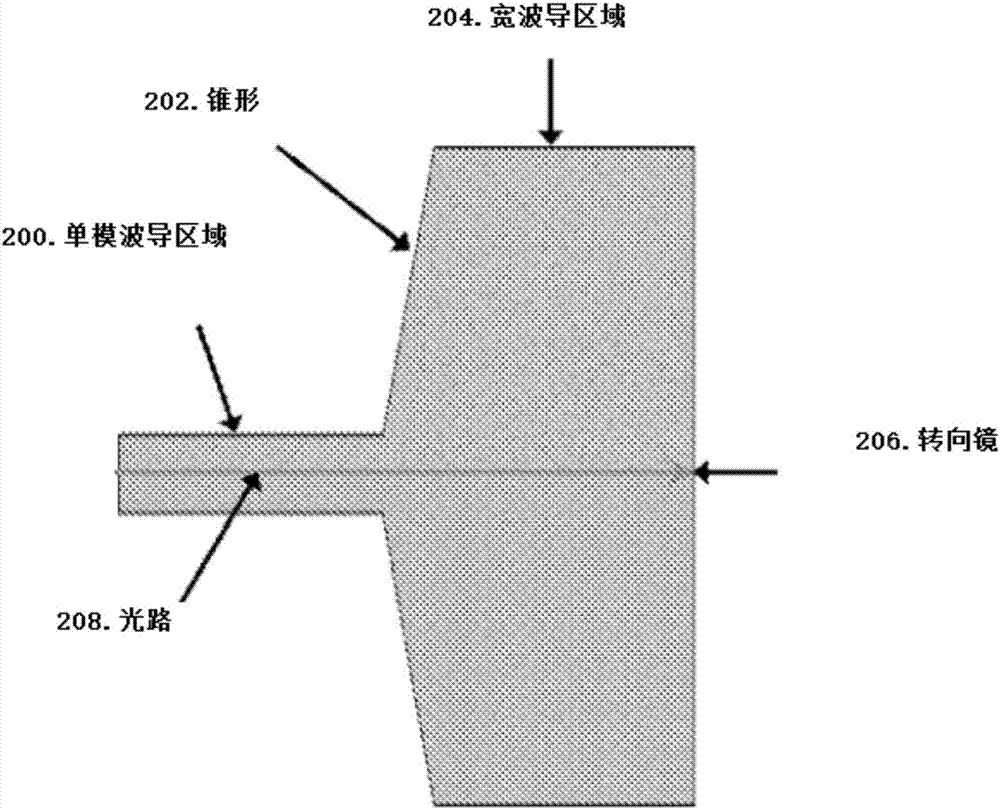
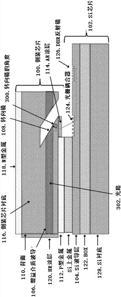
Methods for realizing integrated lasers and photonic integrated circuits on complimentary metal-oxide semiconductor (CMOS)-compatible silicon (Si) photonic chips, potentially containing integrated electronics, are disclosed. The integration techniques rely on light coupling with integrated light coupling elements such as turning mirrors, lenses, and surface grating couplers. Light is coupled from between two or more substrates using the light coupling elements. The technique can realize integrated lasers on Si where a gain flip chip (the second substrate) is bonded to a Si chip (the first substrate) and light is coupled between a waveguide in the gain flip chip to a Si waveguide by way of a turning mirror or grating coupler in the flip chip and a grating coupler in the Si chip. Integrated lenses and other elements such as spot-size converters can also be incorporated to alter the mode from the gain flip chip to enhance the coupling efficiency to the Si chip. The light coupling integration technique also allows for the integration of other components such as modulators, amplifiers, and photodetectors. These components can be waveguide-based or non-waveguide based, that is to say, surface emitting or illuminating.

Description

[0001] Cross References to Related Applications [0002] This application claims the benefit of US Provisional Application No. 62 / 024,379, filed July 14, 2014, which is incorporated herein by reference. technical field [0003] The present invention relates to semiconductor optoelectronic devices, and more particularly to the integration of different optoelectronic devices through optical coupling elements such as turning mirrors, lenses and gratings. Background technique [0004] Silicon (Si) photonics has emerged as an effective photonic integration platform for realizing high-function photonic integrated circuits (PICs) that contain more than one photonic function on a chip. This technology platform enables compact transmitters and receivers for optical communication and sensing applications. Passive components such as but not limited to beam splitters, combiners, arrayed waveguide gratings (AWGs) and echelle gratings can be fabricated in Si with excellent performance an...

Claims


Application Information

Patent Timeline
IPC IPC(8): G02B6/13
CPCG02B6/34G02B6/4214G02B6/12002G02B6/12004G02B6/124G02B2006/12061G02B2006/12078G02B2006/12121H01S3/107H01S5/0085H01S5/021H01S5/026H01S5/0287H01S5/1032H01S5/1085H01S5/141H01S5/142H01S5/4062H01S5/0234H01S5/02255G02B6/13G02B6/14G02B2006/12104G02B2006/12147
Inventor J·克拉姆金S·里斯蒂克
Owner BIOND PHOTONICS
Why Eureka
Try Eureka