An uncooled two-color infrared detector mems chip and its manufacturing method

A technology of an infrared detector and a manufacturing method, which is applied to electric radiation detectors, radiation pyrometry, manufacturing of microstructure devices, etc. or performance reduction, etc., to achieve the effect of extending the working temperature range, good image quality, and expanding the scope of application

Active Publication Date: 2019-01-29
YANTAI RAYTRON TECH
View PDF6 Cites 2 Cited by
  • Summary
  • Abstract
  • Description
  • Claims
  • Application Information

AI Technical Summary

Problems solved by technology

[0005] Due to the different areas where the infrared system is used, the change of climate temperature, the camouflage of the target, the release of infrared decoys, etc., the information obtained by the monochromatic infrared detection system will be weakened.
Especially when the temperature of a moving target changes, the peak wavelength of its infrared radiation will move, which will lead to a significant drop in the detection accuracy of the infrared detector, and may even fail to detect
[0006] In addition, due to the change of the surrounding climate temperature of the uncooled infrared detector, near the high / low temperature working environment (85°C or -40°C), the circuit processing signal is affected by the resistance non-uniformity of the detector or the resistance of the bridge legs, and the imaging quality Or performance will be reduced relative to room temperature imaging

Method used


Image

  • An uncooled two-color infrared detector mems chip and its manufacturing method
  • An uncooled two-color infrared detector mems chip and its manufacturing method
  • An uncooled two-color infrared detector mems chip and its manufacturing method

Examples


Embodiment Construction

[0063] The principle and characteristics of an uncooled two-color infrared detector MEMS chip in the present invention will be described below in conjunction with the accompanying drawings. The given examples are only used to explain the present invention, and are not intended to limit the scope of the present invention.

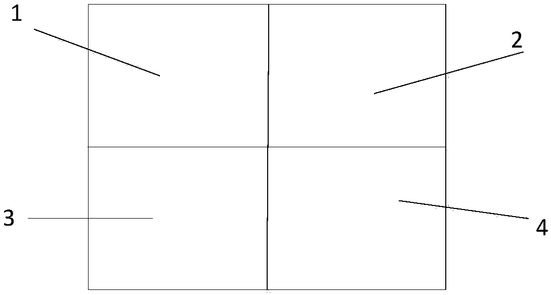
[0064] Such as figure 1 and Figure 15 Shown, a kind of uncooled two-color infrared detector MEMS chip comprises a substrate 5 with ASIC (Application Specific Integrated Circuit: Application Specific Integrated Circuit) and a detector with a micro-bridge support structure, said detector and said The ASIC circuit of the semiconductor substrate 5 is electrically connected, and the detector is divided into four areas arranged in a matrix, which are respectively the first area 1, the second area 2, the third area 3 and the fourth area 4;

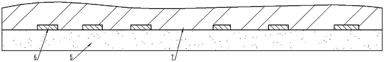
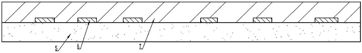
[0065] The detector includes a metal reflective layer 6 and an insulating medium layer 7 on the substrate, the metal reflec...


PUM

PropertyMeasurementUnit
electrical resistanceaaaaaaaaaa

Abstract

The invention relates to an uncooled two-color infrared detector MEMS chip, which is divided into four regions arranged in a matrix: the first and third regions and the second and fourth regions, and the first and third regions are formed with different heights from the second and fourth regions The resonant cavity, and the heat-sensitive layer films with different resistance values ​​are sputtered on it, which can better absorb infrared energy of different bands, and then convert it into electrical signals for processing and image output. The present invention also relates to a method for preparing the above-mentioned chip, including the steps of manufacturing resonant cavities of different heights in the first and third regions and the second and fourth regions respectively, the steps of sputtering the heat-sensitive layer films with different resistance values, and packaging In the step of testing, the chip can work in an ultra-low temperature (-80°C--60°C) environment and an ultra-high-temperature (85°C-100°C) environment.

Description

technical field [0001] The invention relates to an uncooled two-color infrared detector MEMS chip and a manufacturing method thereof, belonging to the field of uncooled infrared detectors. Background technique [0002] Uncooled infrared detectors (uncooled infrared bolometers) have been widely used in civilian fields, such as fire protection, automotive assistance, forest fire prevention, field detection, and environmental protection, in addition to military applications. [0003] The original uncooled infrared focal plane (Uncooled IRFPA) chip is a monochrome chip. At present, there is no two-color infrared detector chip integrated on one chip. The main reason is that different infrared bands require different resonant cavity heights. The traditional process The method and structure cannot be integrated; the square resistance of the vanadium oxide thin film deposited on the monochrome chip is the same value, resulting in a limited operating temperature range. At the end, t...

Claims


Application Information

Patent Timeline
Patent Type & Authority Patents(China)
IPC IPC(8): G01J5/20B81B7/00B81B7/02B81C1/00
CPCB81B7/0009B81B7/02B81C1/00103B81C1/00476G01J5/20G01J2005/0077G01J2005/204
Inventor 甘先锋杨水长王宏臣陈文礼
Owner YANTAI RAYTRON TECH
Why Eureka
Try Eureka